Hi
This is my first project to make my custom PCB.
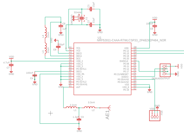
I order my PCB with below schematic and I have a trouble in working with it and I want to know the reason.
I configure my PCB based on below site "Figure 7. CAAA WLCSP 2-layer setup"
https://docs.nordicsemi.com/bundle/ps_nrf52811/page/ref_circuitry.html
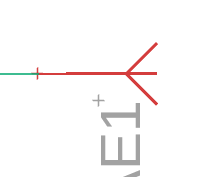
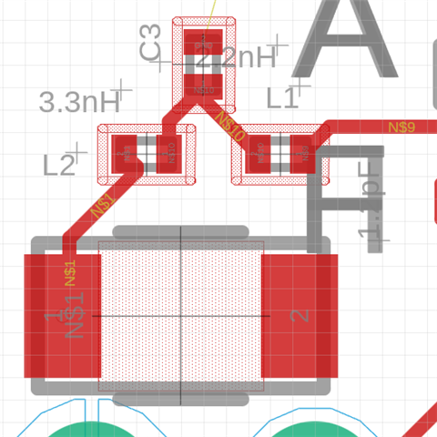
For now what I found wrong is I didn't connect my antenna to gnd. But in schematic there is only 1 pinout so I not sure this is actual problem... (But in PCB board it has 2 pinout)
But even though it causes an error, is it matter to whole nrf52811 circuit configuration. Is it should be only my Bluetooth function doesn't work with this error?
So my current situation is when I connect my nrf52811 swdio, swdclk pinout with nrf52840 DK I think my code is uploaded to nrf52811 socs not nrf2840. (because DK board doesn't change)
(I tried to upload code with below site configuration. https://docs.nordicsemi.com/bundle/ug_nrf5340_dk/page/UG/dk/ext_programming_support_P20.html)
(SWDIO, SWDCLK, VTG, and I power my PCB board with DK vdd pinout)
I want to check my board working by connecting LED to pin 5.
If there is any additional info needed please tell me I will reply as soon as possible.
Sorry for my complex question, any advice would be helpful for me. Thank You!


