Hello
I’m using the NINA-B306-00B BLE module which uses the nRF52840 MCU for a custom board application. The BLE module interacts with two sensors, an accelerometer via SPI and a barometer via I2C. I also have a battery voltage monitoring circuit which uses a digital pin to turn on a NFET and an analog pin to measure voltage.
I am writing to verify that the selected GPIO pins will not cause conflicts or interfere with the proper operation of SPI, I2C, or ADC functionalities. Specifically, I want to ensure that these pin assignments will not lead to resource conflicts, signal integrity issues, or necessitate the use of bit-banging as a workaround.
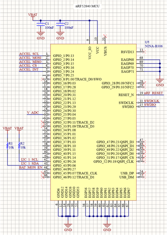
For my accelerometer, I’m using pins GPIO_1, GPIO_2, GPIO_3, GPIO_4 & GPIO_5 for ACCEL_SCL, ACCEL_MOSI, ACCEL_MISO, ACCEL_CS & ACCEL_INT respectively.
For my pressure sensor, I’m using pins GPIO_42 & GPIO_43 for SCL & SDA respectively. For my battery voltage monitoring circuit, I’m using pins GPIO_44 & GPIO_25 for BAT_MON_EN and V_ADC respectively.
I've attached an image of the connections to my mcu below for reference.
My reasoning for choosing all the specific GPIO pins mentioned above is because they aren’t radio sensitive so I’m not limited to keep the frequencies below 10 kHz, and only use standard drive strength on these digital pins. GPIO_25 is analog capable.
NB: Both the sensors and my MCU operate at the same VDD
Thanks

