Hi
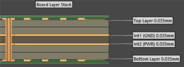
We use the nRF52840 (aQFN73) with a 4-layer 1.6 mm PCB for our current project. The top and bottom layers are for signals, the two internal layers are ground and power planes.
The reference design connects inner signals to the midlayer with a blind via. I've placed a vias in pads from the top layer to the bottom layer. Can I use a 0.2 mm drill size for the vias instead of 0.1 mm, which is used in the reference design? The aim is to reduce costs and increase the number of producers.
Has anyone experience with the same layer stack?

Best regards,
Michael

