Hello,
It has been a while since I have done any controlled impedance and was wondering if someone could provide me a quick sanity check before I continue:
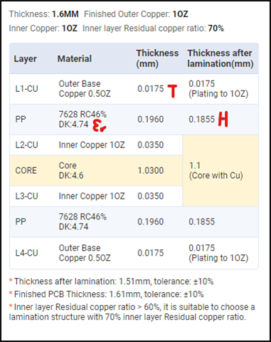
Here is the board stack up. I am using the top copper(L1) as waveguide and L2 as ground:

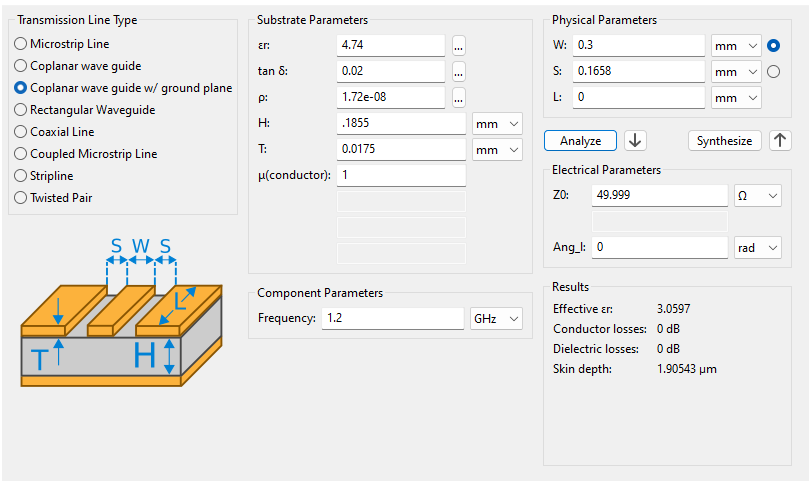
Here is the calculation. Chose 0.3mm trace width to keep manufacturing costs low.

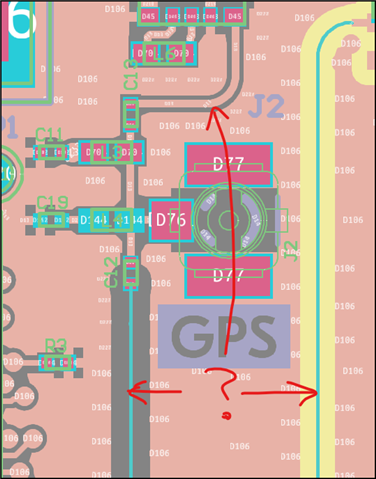
It looks fine to me but after looking at the DK I am starting to question myself. First question is, the 50 Ohm trace is very thin and then transitions to a thicker trace. Do I need to be transitioning trace widths too?
Second question, the GERBER file from the DK shows that there is ground immediately below on layer 2 meaning the "H" parameter should be relatively close to my calculation. How did the DK get the trace width W=0.1mm and Spacing S=0.41? To get those values using KiCad's calculator, you need a very thick board.


