DevAcademy NrfConnect Intermediate Course, lesson 5 exercise 2 hookups?

Hello,

I am going through the intermediate DevAcademy tutorials right now because I specifically need to use the 52840 dev kit to interface with a SPI driven ili9340 device. What I have is adafruit's 480x320 TFT featherwing and you guys helpfully provide an exercise where you print stuff out on adafruit's 2.8" LCD shield. I figured that the change in screen size would be fairly trivial, maybe a little fuckery in the configs and we are good. The problem is that I ended up kinda baffled by how you hookup the LCD shield to adafruit. I am relatively familiar with SPI hookups on other platforms. MISO, MOSI, CS and SCK and you a good to go. Daisy chain things together using different CS GPIO to control multiple slave devices. Pretty straight forward as far as hook ups are concerned. However the way you do it in the exercise you plug the LCD shield directly onto the 6 pin header in the middle of the Devkit and I can't seem to wrap my head around how that makes sense. What confuses me is:

A) How are you powering the LCD screen here? There is no GND Pin. I feel kinda silly for even asking that but for some reason I genuinely can't figure this out.

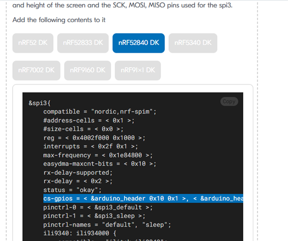
B)What are you using as CS? I don't see where it's defined anywhere in the exercise. Is it the "Detect" pin? Where is that defined and how do you reference that GPIO in any other context?

C) What is the Reset pin for? Just in case you need to reset the LCD screen?

Question B is kinda that important part here. I need to know how to define CS and I am just not seeing where, in this exercise, that's happening. I would really appreciate if you could clairfy this for me. I feel like I am missing something obvious but I am nearing the end of my rope.

Thanks.

  • Hello,

    Other than that I would change:

    compatible = "ilitek,ili9341";
    to 
    compatible = "ilitek,ili9340";
    but other than that, I don't see anything in the exercise that points to anything ili9341 specific.

    A) How are you powering the LCD screen here? There is no GND Pin. I feel kinda silly for even asking that but for some reason I genuinely can't figure this out.

    The layout on these boards is called an "Arduino header", or "Arduino Shield". Basically what it means is that the spacing is standardized, as well as the functionality of some particular pins. If you look closely in the picture, there are a lot more pins than those 6 that are connected when you set the PCB on top of the DK, including a bunch of normal GPIOs, and VDD and GND.

    B)What are you using as CS? I don't see where it's defined anywhere in the exercise. Is it the "Detect" pin? Where is that defined and how do you reference that GPIO in any other context?

    I agree that this is not obvious. But the CS pins are defined here:

    The first one for the "ili" and the second one for the tft touch.

    When it says: &arduino_header 0x10 0x1, and I know it is for the nRF52840 DK, I usually start looking in the nrf52840dk_nrf52840.dts file. There you can find:

    	arduino_header: connector {
    		compatible = "arduino-header-r3";
    		#gpio-cells = <2>;
    		gpio-map-mask = <0xffffffff 0xffffffc0>;
    		gpio-map-pass-thru = <0 0x3f>;
    		gpio-map = <0 0 &gpio0 3 0>,	/* A0 */
    			   <1 0 &gpio0 4 0>,	/* A1 */
    			   <2 0 &gpio0 28 0>,	/* A2 */
    			   <3 0 &gpio0 29 0>,	/* A3 */
    			   <4 0 &gpio0 30 0>,	/* A4 */
    			   <5 0 &gpio0 31 0>,	/* A5 */
    			   <6 0 &gpio1 1 0>,	/* D0 */
    			   <7 0 &gpio1 2 0>,	/* D1 */
    			   <8 0 &gpio1 3 0>,	/* D2 */
    			   <9 0 &gpio1 4 0>,	/* D3 */
    			   <10 0 &gpio1 5 0>,	/* D4 */
    			   <11 0 &gpio1 6 0>,	/* D5 */
    			   <12 0 &gpio1 7 0>,	/* D6 */
    			   <13 0 &gpio1 8 0>,	/* D7 */
    			   <14 0 &gpio1 10 0>,	/* D8 */
    			   <15 0 &gpio1 11 0>,	/* D9 */
    			   <16 0 &gpio1 12 0>,	/* D10 */
    			   <17 0 &gpio1 13 0>,	/* D11 */
    			   <18 0 &gpio1 14 0>,	/* D12 */
    			   <19 0 &gpio1 15 0>,	/* D13 */
    			   <20 0 &gpio0 26 0>,	/* D14 */
    			   <21 0 &gpio0 27 0>;	/* D15 */
    	};

    So the &arduino_header 0x10 means the 0x10th element = 16th element, which is gpio1 12 = P1.12. 

    &arduino_header 0xa = 10th element = P1.05.

    The final parameter is active high/low. 

    C) What is the Reset pin for? Just in case you need to reset the LCD screen?

    Not sure if it is used, but in that case, yes. It would reset the shield, so that when the application boots up, sending the init commands to the shield, they are in the same default state.

    Question B is kinda that important part here. I need to know how to define CS and I am just not seeing where, in this exercise, that's happening. I would really appreciate if you could clairfy this for me. I feel like I am missing something obvious but I am nearing the end of my rope.

    When you declare an SPI device like this, it is always the cs-gpios that are the cs gpios. You can pick one from the arduino header from the boards dts file, but you can also write it directly, like it is done in lesson 5 exercise 1:

    &i2c0 {	status = "disabled";};
    &spi0 {	status = "disabled";};
    &i2c1 {	status = "disabled";};
    	
    &spi1 {
        compatible = "nordic,nrf-spi"; //using SPI as per ERRATA 58
        status = "okay";
        pinctrl-0 = <&spi1_default>;
        pinctrl-1 = <&spi1_sleep>;
        pinctrl-names = "default", "sleep";
        cs-gpios = <&gpio0 30 GPIO_ACTIVE_LOW>;
        bme280: bme280@0 {
        	compatible = "bosch,bme280";
        	reg = <0>;
            spi-max-frequency = <1000000>; 
        };
    };

    <&gpio0 30 GPIO_ACTIVE_LOW>; means P0.30, active low. 

    Best regards,

    Edvin

  • thank you so much. This is extremely helpful.

Related