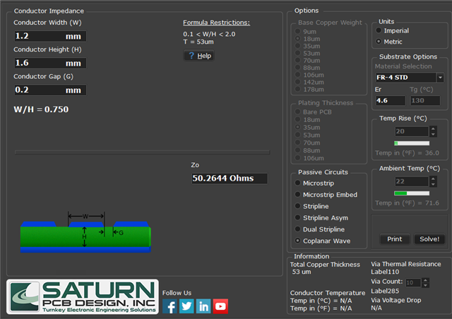
I need to match the 50 ohm impedance for antenna performance.
It would be easier to manufacture using 4 layers, but I'm planning to manufacture it in 2 layers due to cost issues.
When I calculated it with an impedance calculator when manufacturing in 2 layers, the width was too wide at about 3 mm.
When I searched for several boards, I saw a case where an nrf52840 board was manufactured in 2 layers.
However, the width was not as wide as 3 mm.
Is there any know-how to manufacture an nrf52840 board in 2 layers without reducing the Bluetooth antenna performance?
Is there a sample file of a PCB manufactured in 2 layers?
Thank you.