Hello,
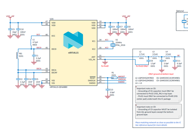
I am designing a PCB using the nRF54L15 and a ceramic antenna and got confused regarding the impedance-matching network. In the detasheet a 1.5pF, 2.0pF, and 0.3pF capacitors and 2.7nH and 3.5nH inductors are used, but in the DK schematics an additional 1.4pF parallel capacitor is added before the PCB trace antenna. I also have a different circuit suggested in the antenna datasheet. How should I connect my ceramic antenna to the MCU?
Also, according to the nRF54L15 datasheet the matching network should be grounded only to the ground pad and bottom layer, but it is not the case in the DK schematics.
Best regards,
Amine