I have made my own NRF52832 Dev board as in the next image:
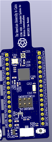
I received the board, and ICs and hand-soldered them in my home.
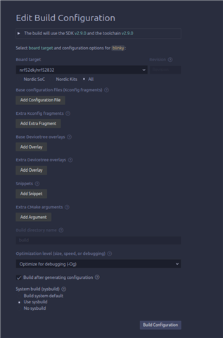
however, I am still a newbie in nRF SDK, I started watching https://academy.nordicsemi.com/courses/nrf-connect-sdk-fundamentals/ video series, I have followed along, used blinky app as in the course and entered the following build configuration for the board:
after the build was successful, I used the "merged.hex" output file and I am trying to download it manually into the board using a j-link.
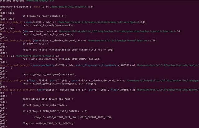
here is the log of me trying to download the code onto the board:
License(s): FlashBP, GDB
USB speed mode: Full speed (12 MBit/s)
VTref=3.295V


Type "connect" to establish a target connection, '?' for help
J-Link>connect
Please specify device / core. <Default>: NRF52832_XXAA
Type '?' for selection dialog
Device>
Please specify target interface:
  J) JTAG (Default)
  S) SWD
  T) cJTAG
TIF>S
Specify target interface speed [kHz]. <Default>: 4000 kHz
Speed>
Device "NRF52832_XXAA" selected.


Connecting to target via SWD
InitTarget() start
InitTarget() end - Took 2.90ms
Found SW-DP with ID 0x2BA01477
DPIDR: 0x2BA01477
CoreSight SoC-400 or earlier
Scanning AP map to find all available APs
AP[2]: Stopped AP scan as end of AP map has been reached
AP[0]: AHB-AP (IDR: 0x24770011)
AP[1]: JTAG-AP (IDR: 0x02880000)
Iterating through AP map to find AHB-AP to use
AP[0]: Skipped. Could not read AHB ROM register
AP[1]: Skipped. Not an AHB-AP
Attach to CPU failed. Executing connect under reset.
DPIDR: 0x2BA01477
CoreSight SoC-400 or earlier
Scanning AP map to find all available APs
AP[2]: Stopped AP scan as end of AP map has been reached
AP[0]: AHB-AP (IDR: 0x24770011)
AP[1]: JTAG-AP (IDR: 0x02880000)
Iterating through AP map to find AHB-AP to use
AP[0]: Core found
AP[0]: AHB-AP ROM base: 0xE00FF000
CPUID register: 0x410FC241. Implementer code: 0x41 (ARM)
Found Cortex-M4 r0p1, Little endian.
Cortex-M: The connected J-Link (S/N 801045859) uses an old firmware module: V1 (current is 2)
FPUnit: 6 code (BP) slots and 2 literal slots
CoreSight components:
ROMTbl[0] @ E00FF000
[0][0]: E000E000 CID B105E00D PID 000BB00C SCS-M7
[0][1]: E0001000 CID B105E00D PID 003BB002 DWT
[0][2]: E0002000 CID B105E00D PID 002BB003 FPB
[0][3]: E0000000 CID B105E00D PID 003BB001 ITM
[0][4]: E0040000 CID B105900D PID 000BB9A1 TPIU
[0][5]: E0041000 CID B105900D PID 000BB925 ETM
Memory zones:
  Zone: "Default" Description: Default access mode
Cortex-M4 identified.
J-Link>loadfile C:\Users\User\Downloads\merged.hex
'loadfile': Performing implicit reset & halt of MCU.
Reset: Halt core after reset via DEMCR.VC_CORERESET.
Reset: Reset device via AIRCR.SYSRESETREQ.
Downloading file [C:\Users\User\Downloads\merged.hex]...

****** Error: Failed to preserve target RAM @ 0x20000000-0x2000FFFF.
Failed to prepare for programming.
Unspecified error -1
J-Link>
I don't know what "Error: Failed to preserve target RAM @ 0x20000000-0x2000FFFF." mean but what makes me sure the IC is working is that I can halt the CPU and get the registers content as in the following log:
J-Link>halt
PC = EFFFFFFE, CycleCnt = 00000000
R0 = 00000000, R1 = 00000000, R2 = 00000000, R3 = 00000000
R4 = 00000000, R5 = 00000000, R6 = 00000000, R7 = 00000000
R8 = 00000000, R9 = 00000000, R10= 00000000, R11= 00000000
R12= 00000000
SP(R13)= FFFFFFFC, MSP= FFFFFFFC, PSP= 00000000, R14(LR) = 7FFFFFFF
XPSR = FFFFFFFE: APSR = NZCVQ, EPSR = 0700FC00, IPSR = 01E (INTISR14)
CFBP = 00000000, CONTROL = 00, FAULTMASK = 00, BASEPRI = 00, PRIMASK = 00

FPS0 = 00000000, FPS1 = 00000000, FPS2 = 00000000, FPS3 = 00000000
FPS4 = 00000000, FPS5 = 00000000, FPS6 = 00000000, FPS7 = 00000000
FPS8 = 00000000, FPS9 = 00000000, FPS10= 00000000, FPS11= 00000000
FPS12= 00000000, FPS13= 00000000, FPS14= 00000000, FPS15= 00000000
FPS16= 00000000, FPS17= 00000000, FPS18= 00000000, FPS19= 00000000
FPS20= 00000000, FPS21= 00000000, FPS22= 00000000, FPS23= 00000000
FPS24= 00000000, FPS25= 00000000, FPS26= 00000000, FPS27= 00000000
FPS28= 00000000, FPS29= 00000000, FPS30= 00000000, FPS31= 00000000
FPSCR= 00000000
J-Link>
UPDATE: I upgraded J-link firmware and got this error (it seems the same thing but more specific):
J-Link>loadfile C:\Users\User\Downloads\merged2.hex 'loadfile': Performing implicit reset & halt of MCU. Reset: Halt core after reset via DEMCR.VC_CORERESET. Reset: Reset device via AIRCR.SYSRESETREQ. Downloading file [C:\Users\User\Downloads\merged2.hex]... ****** Error: Verification of RAMCode failed @ address 0x200000A4. Write: 0xBDF21C18 F0009800 Read: 0x5DF21C18 F0009800 Failed to prepare for programming. Failed to download RAMCode! Unspecified error -1
I tried command 'nrfjprog --recover' and got the following response
Recovering device. This operation might take 30s.
Erasing user code and UICR flash areas.
then used the command 'nrfjprog -f NRF52 --program merged.hex --sectorerase'
and got the response:[ #################### ] 0.323s | Erase file - Done erasing [error] [ nRF52] - The write access failed, but no cause could be determined. [error] [ nRF52] - It may be due to an unaligned access, accessing a nonexistent memory, or a communication issue. [error] [ nRF52] - Failed while performing 'Write' operation on target address 0x00000000. -102: An unknown error. [error] [ nRF52] - Failed while reading device information. [error] [ Client] - Encountered error -102: Command program_file executed for 374 milliseconds with result -102 [error] [ Worker] - An unknown error. ERROR: JLinkARM DLL reported an error. Try again. If error condition ERROR: persists, run the same command again with argument --log, contact Nordic ERROR: Semiconductor and provide the generated log.log file to them. NOTE: For additional output, try running again with logging enabled (--log). NOTE: Any generated log error messages will be displayed. PS C:\Users\User\Downloads> nrfjprog --recover Recovering device. This operation might take 30s. [error] [ JLink] - DAP error while reading AIRCR. Erasing user code and UICR flash areas.
I tried to write and read into RAM memory region and it was successful:
I then tried to do the same for Flash, I couldn't read memory on the first trial, and then on the second trial I could read it successfully. I don't know what may cause that.
J-Link>Mem8 0x0000000020000000
Syntax: mem8 <Addr>, <NumBytes>
J-Link>Mem8 0x0000000020000000, 2
20000000 = 6F 8D
J-Link>Write1 0x0000000020000000, 0xff
Writing FF -> 20000000
J-Link>Mem8 0x0000000020000000, 2
20000000 = FF 8D
J-Link>Mem8 0x0000000000000000,2
00000000 = 80 16
J-Link>Write1 0x0000000000000000, 0xff
Writing FF -> 00000000
J-Link>Mem8 0x0000000000000000,2
Could not read memory.
J-Link>Mem8 0x0000000000000000,4
00000000 = FF 16 00 20
J-Link>Mem8 0x0000000000000000,2
00000000 = FF 16
J-Link>
another update, as shown in the image, it seems as if it works with my black magic probe but doesn't work with my segger j-link: