Hardware review

hi all

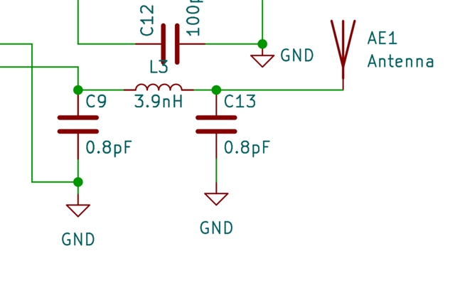
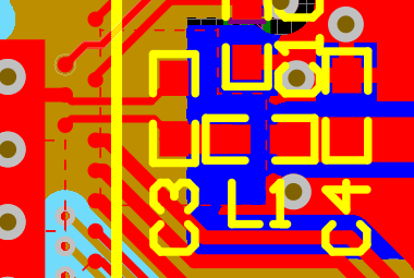
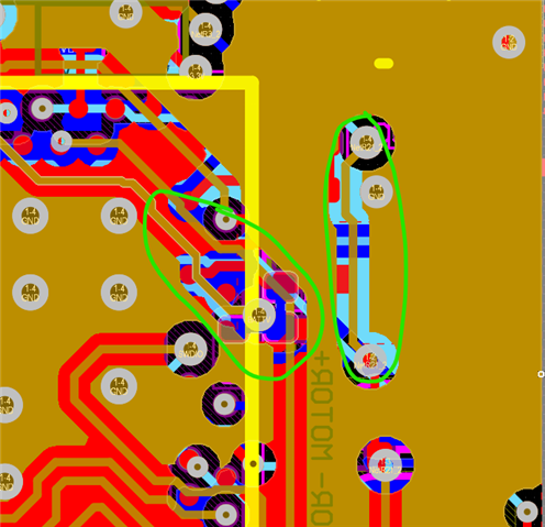
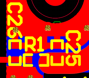
I designed this board. Could you please review it from a hardware perspective, especially regarding the nRF52840 microcontroller? Specifically, I would like feedback on the antenna-related aspects.

Also, the schematic and PCB files are attached.

schematic:

https://www.dropbox.com/scl/fi/xz16orcoytdqy1ll0z0iy/schver3.pdf?rlkey=zmq35ubbf9nzhe1ig8pwisomr&st=mhcvdhbf&dl=0

PCB:

https://www.dropbox.com/scl/fi/ijf5dxkydopjps24hmddn/SchVer3.PcbDoc?rlkey=b0niehacfs8bbkdk101aqen24&dl=0

thank you very much

Parents
  • My only comment: check whether you can leave VREF on your DRV8214 driver IC unconnected like that.

    i had issues with a DRV8411A not working as expected when I inadvertently left VREF unconnected.

    Also, there are better ways to monitor battery voltage that don't put a constant load on the battery like you have with your 2 x 100k resistors. But if you're not aiming for super low standby current, it's probably not an issue.

  • thank you, i use Vref as internal reference

    what is your comment about antenna?

    is it matching network true?

  • Can't really comment on your matching network. If you've followed the design on the nRF52840 DK in terms of antenna layout and matching network, you'll more than likely have something that works. Whether it's compliant or not, you'll have to do the testing to confirm.

    I've got a very similar matching network on all my nRF52832 designs:

  • Hi,

    The nRF52840 part of your schematic looks good.

    There are however multple issues with the layout:

    • C24 must only be grounded to the VSS_PA pin and the center GND pad, this is done to improve the filter performance at the 2nd harmonic frequency. Here is a snippet from the reference layout that show the correct way to ground this capacitor:
    • There must be only GND directly under the RF path, matching networks and transmission line, so these traces on the 2nd layer must be moved:
    • The layout of the antenna matching network is very messy, and must be simplified. It is very important that the components are place close to each other, and the traces between them are keep as short as possible. Since there is very little room on this board I recommend you switch to using 0201 components for the antenna and radio matching networks. This will allow you to mount the components like on the nRF52840 dongle:
    katrindqaws said:

    what is your comment about antenna?

    is it matching network true?

    The antenna looks good.

    The values of the antenna matching network must be determined by measuring the antenna impedance after the board is produced. We have a paper on the antenna matching network tuning process:

    https://docs.nordicsemi.com/bundle/nwp_017/resource/nwp_017.pdf

    If you don't have the equipment needed for tuing the antenna, you can open a private ticket once your board is produced and we will help you with tuning.


    Best regards,

    Bendik

Reply
  • Hi,

    The nRF52840 part of your schematic looks good.

    There are however multple issues with the layout:

    • C24 must only be grounded to the VSS_PA pin and the center GND pad, this is done to improve the filter performance at the 2nd harmonic frequency. Here is a snippet from the reference layout that show the correct way to ground this capacitor:
    • There must be only GND directly under the RF path, matching networks and transmission line, so these traces on the 2nd layer must be moved:
    • The layout of the antenna matching network is very messy, and must be simplified. It is very important that the components are place close to each other, and the traces between them are keep as short as possible. Since there is very little room on this board I recommend you switch to using 0201 components for the antenna and radio matching networks. This will allow you to mount the components like on the nRF52840 dongle:
    katrindqaws said:

    what is your comment about antenna?

    is it matching network true?

    The antenna looks good.

    The values of the antenna matching network must be determined by measuring the antenna impedance after the board is produced. We have a paper on the antenna matching network tuning process:

    https://docs.nordicsemi.com/bundle/nwp_017/resource/nwp_017.pdf

    If you don't have the equipment needed for tuing the antenna, you can open a private ticket once your board is produced and we will help you with tuning.


    Best regards,

    Bendik

Children
No Data
Related