nRF7002 layout details

Dear Nordic,

I am currently integrating nRF7002 into one of the hardwares. I am trying to make the PCB as compact as possible so it looks amendment to the reference layout is inevitable. There are some details on layout that I would like to confirm before I conduct practical changes.

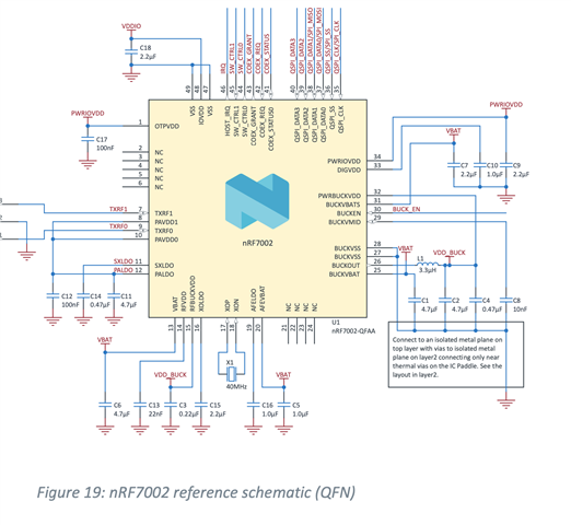
QFN package is my choice, below is the screenshot of the QFN reference circuit from product specification:

My questions are:

1) What is the actual maximum current that goes through L1 inductor? So I can know if I had a chance to use a smaller inductor form factor.

2) C8 decoupling capacitor on BUCKVMID pin. How sensitive this pin is to PCB parametric? As I may need to move C8 to another side of PCB but I am not sure how much the so-introduced capacitance due to extra via that may impact.

3) X1 crystal. This crystal's spec states its load capacitor is 8pF. Though I did not find the presence of load capacitors in circuit. Is that because the load caps are integrated in nRF7002 or in the crystal? This part is not very available in my local supply channels so I may need to find an alternative part. Should 8pF caps then be presented for other parts?

Many thanks.

/Roland

  • 1) What is the actual maximum current that goes through L1 inductor? So I can know if I had a chance to use a smaller inductor form factor.

    You want to use a smaler inductor, but in size/dimensions only ? not value?

    2) C8 decoupling capacitor on BUCKVMID pin. How sensitive this pin is to PCB parametric? As I may need to move C8 to another side of PCB but I am not sure how much the so-introduced capacitance due to extra via that may impact.

    This should be ok as long as its not moved to far away. 

    But, I want to note that we higly recommend that you follow the reference layout that we have as best as possible.


    3) X1 crystal. This crystal's spec states its load capacitor is 8pF. Though I did not find the presence of load capacitors in circuit. Is that because the load caps are integrated in nRF7002 or in the crystal? This part is not very available in my local supply channels so I may need to find an alternative part. Should 8pF caps then be presented for other parts?

    Strongly recommend you to source the crystal that we use or one with similar specs. Using something else will be difficult and limited help that we can provide. The load caps are internal. 


    Regards,
    Jonathan

  • Thank you @JONATHAN

    1) What is the actual maximum current that goes through L1 inductor? So I can know if I had a chance to use a smaller inductor form factor.

    You want to use a smaler inductor, but in size/dimensions only ? not value?

    Yes, I mean smaller in size, not value. 

    Of course, if a smaller value inductor can be used here instead, that can also lead to the reduction in size when choosing inductor. 

    Any hints will be appreciated.

  • rolandash said:
    Yes, I mean smaller in size, not value. 

    You will need to stick to the value given. 

    What sometimes can be done in similar situations is to use two inductors in series that total the same value. I have not seen this been done with this L1 inductor so I am not sure how well it will work. But in theory it should work. 

    I will check internally if we have any other recommendations. 

    Regards,
    Jonathan

  • Thanks for that @Jonathan.

    And about the X1 and load caps, I am trying to find alter part with exactly the same spec.

    The load caps are internal. 

    Are these load caps embedded in nRF7002 chip, or in X1 crystal? 

Related