
Hello,
NCS 2.9.0
nRF54L15 DK 0.9.1
I am trying to follow the instructions in the manual in the User Guide of the nRF54L15 DK to use P1.00 and P1.01 as normal GPIOs.
(side note: there is a typo in section 2.6 in the manual XL1 and XL2 are not on P0.00 and P0.01, but instead on P1.00 and P1.01)
I cut colder bridges SB3 and SB4, and soldered SB5 and SB6.
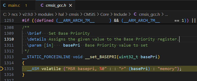
However, when I try running and debug blinky, I get an error in cmsis_gcc.h on boot.
If I deactivate the clock node in the device tree overlay, I can run blinky again.
&clock {
  status = "disabled";
};
However, I still do not get any output on P1.00 and P1.01.
What setting am I missing?

