NRF5340 custom Board Schematic Review

Hi , We as a Budding Tech startup are developing a Product With NRF5340-CLAA chip.
We made the design referring the Datasheet and Reference designs provided by Nordic Semiconductor.
But we still need a Proper Schematic Review of our Design (Especially the MCU part), so that to make sure we did not miss anything.
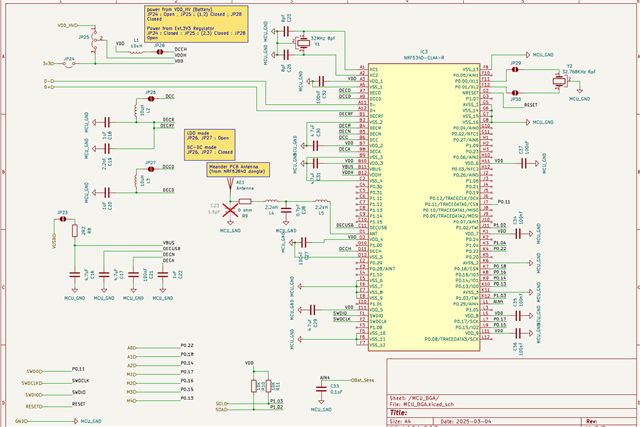
i am attaching our Schematic to be reviewed in this Post.

Quick Overview of the Schematic
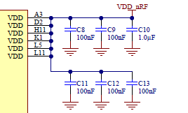
- NRF5340-CLAA IC
- Flexible Power scheme (Used jumpers where ever needed to switch between multiple Power Configurations)
- Meander PCB antenna from NRF52840 dongle
- Can be Powered from Battery directly (VDDH) or External 3.3V (included jumpers to switch the configuration)
- Jumper to Enable and disable the DC-DC inductors
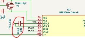
- Jumpers for 32.768KHz Crystal

Questions:

1. do we need external Load capacitors for 32MHz and 32.768Khz oscillators ?
2. is 32.768KHz Crystal Mandatory
3. does the flexible Power scheme made with Jumpers  Look good ?

MM_V1.3.0_Prototype_Schematic_MCU.pdf

Parents
  • Hi Surya,

    1. do we need external Load capacitors for 32MHz and 32.768Khz oscillators ?

    For the 53 series, you have the option of using internal or external capacitors. So it's not necessary to use external capacitors.

    2. is 32.768KHz Crystal Mandatory

    No it's not. As mentioned in the reference design, it's optional. Required only when you need higher precision or accuracy. Or when you use ANT/ANT+ applications.

    3. does the flexible Power scheme made with Jumpers  Look good ?

    It looks fine and is okay as long as you use them appropriately. Also, make sure that the VDD rail is not externally powered when you go for the HV mode, since it is then an output and not input.

    I would suggest you to take a look at the General PCB guidelines for nRF53 when creating a custom product using the nRF5340.


    Now regarding your schematics:

    1. Here, the value used in the reference design is 1uF, which would be a 1000nF:

    Also, I see that you have 4.7uF connected to various VDD pins, which is not correct and I think you might need 1uF(you can check the reference design).

    3. Also, the connections to the other VDD pins need to be as shown in the reference design as follows:


    You need to connect VDD pins to five 100nF each and a 1uF, whereas you seem to have connected 6 caps of 100nF. So it looks like you are missing a 1uF in your VDD connections.

    4.Also, for the antenna, please make sure you have an antenna matching component before connecting the antenna. Details regarding this can be found in the PCB Guide link that I have attached earlier.

    On the whole, I would suggest you to keep all component values and connections similar to the reference design for proper outcome.

    Regards,

    Priyanka

  • Thank You   for the Brief Review. 
    We shall work on the points mentioned
    Thank you

Reply Children
No Data
Related