Hi ,
We are developing a product with NRF5340-CLAA-R WLCSP package IC.
While entering the PCB design stage we encountered an Issue with its footprint.
First we imported Footprint Models from Digikey, and SamacSys (Mouser and Arrow)
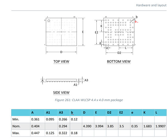
the PCB land Pads size for the chip in these Models seems different than the One in the Altium Reference design files provided by Nordic.
Here are the differences Observed
1. Nordic Reference Layout Altium Files : pad size = 0.17mm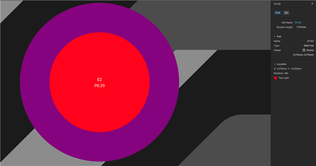
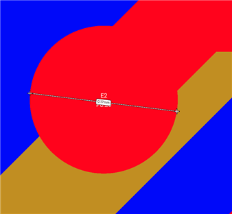
2. Digikey Provided Footprint Model (KiCAD) : pad size = 0.1524mm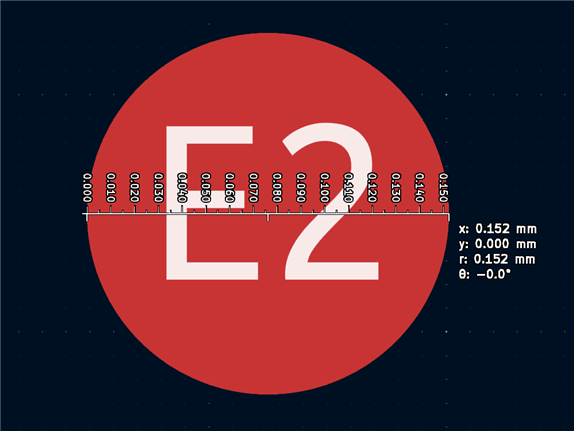
3. Mouser and Arrow Provided Footprint Model from SamacSys (KiCAD) : pad size = 0.148mm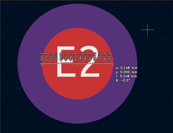
Mouser, Arrow and Digikey claims that their Models are Trusted By Community
Can anyone Experience with NRF5340-CLAA chip Hardware design Clarify on which one was correct and will there be any Issue in Using Digikey, Mouser and Arrow Models.
Models provided by Digikey, Mouser and Arrow were handy, since they make Development Faster instead of Creating Models from Scratch. We would really like to use those models and never had an issue with Other models of Parts.
Any Help regarding this really appreciated.
Thank You