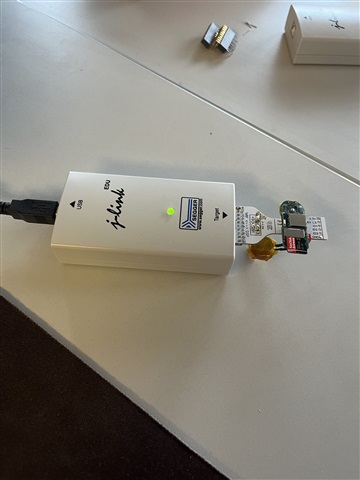
Hi, I am seeking assistance with a very weird issue encountered while programming an nRF5340 SoC using a custom debugging-PCB using a SEGGER J-Link EDU debugger.
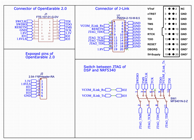
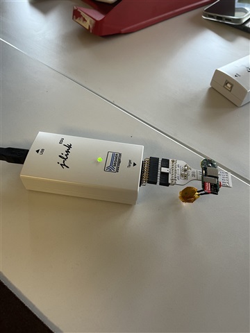
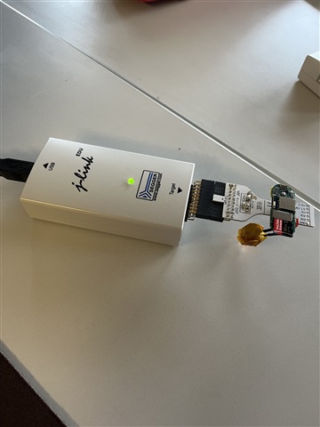
The debugging PCB is designed to plug directly into the J-Link (and the board featuring the nRF5340 plugs into this board).
The nRF appears in VS Coder under connected devices, but attempts to flash the device result in the following error:
[error] [ Client] - Encountered error -102: Command program_file executed for 755 milliseconds with result -102
[error] [  nRF53] - The write access failed, but no cause could be determined.
[error] [  nRF53] - It may be due to an unaligned access, accessing a nonexistent memory, or a communication issue.
[error] [  nRF53] - Failed while performing 'Write' operation on target address 0x01000000.
-102: An unknown error.
[error] [  nRF53] - Failed while reading device information.
[error] [ Worker] - An unknown error.
ERROR: JLinkARM DLL reported an error. Try again. If error condition
ERROR: persists, run the same command again with argument --log, contact Nordic
ERROR: Semiconductor and provide the generated log.log file to them.
NOTE: For additional output, try running again with logging enabled (--log).
NOTE: Any generated log error messages will be displayed.
FATAL ERROR: command exited with status 33: nrfjprog --program /Users/philipp/TECO/open-earable-v2/build_1/merged_CPUNET.hex --sectorerase --verify -f NRF53 --coprocessor CP_NETWORK --snr 260115464
HOWEVER, when the debugging PCB is not plugged directly into the J-Link, but each pin is individually connected to the J-Link using jumper wires, programming proceeds without issues.
I've narrowed down the issue to the SWCLK line: connecting the debugging PCB directly and soldering a 5 cm jumper wire between the SWCLK pins solves the issue.
This doesn't work:
This does work:
This doesn't work again:
Troubleshooting Steps Undertaken:
1. Measured the resistance of the connecting cable, which is approximately 0.5 Ω
2. Introduced resistors ranging from 0.5 ohms to 200 Ω in series with each J-Link pin (especially SWCLK to simulate the jumper wire resistance); this did not resolve the issue.
3. I noticed that probing the SWCLK line with an oscilloscope prevents successful flashing, indicating sensitivity on this line.
4. Implemented external pull-up and pull-down resistors for SWDIO and SWCLK , as well as low-pass filters, without achieving successful programming.
5. Built an "extension" plug that plugs directly into the J-Link and then in the debugging PCB, then it doesn't work. If the debugging board is not entirely plugged in all the way (leaving some millimetres while ensuring all lines are connected, it works....
When probing the lines with an oscilloscope, you can see a bit of ringing, but the signal is the same if probed with jumper wire extensions or without, so this can't be the issue, right?
TLDR: I'm literally clueless at this point. All my colleagues have looked over the schematics, we ruled out any issues we've come up with, it just doesn't work, when there's a direct connection, it works when there a jumper wire in the SWCLK line
I appreciate any insights or recommendations from the community to resolve this weird bug