nrf52840 DK description and schematic do not agree for external debug port P19

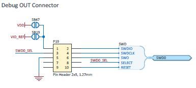
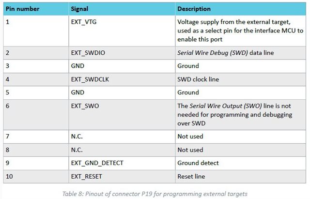
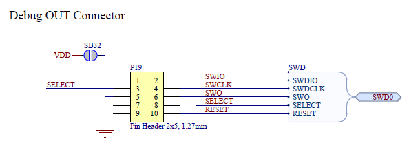
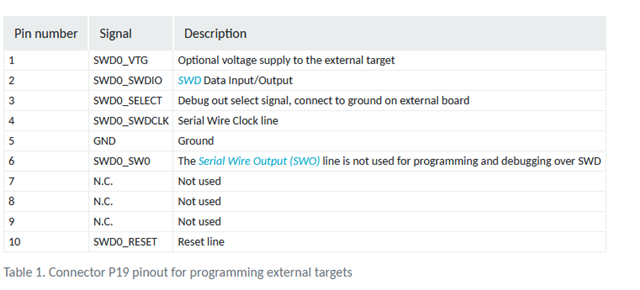
I am attempting to connect my nrf52840/52811 DK to my custom PCB that contains nrf52840. The DK users guide describe the connections on the P19 debug out port but I can see on the schematic for the DK that something is incorrect. Specifically, the UG says that Pin1 is "EXT_VTG" and is used to select this port for debugging by connecting a 3V level. The schematic shows pin1 as an optional "power out" to my custom PCB and is not connected to anything if I don't short one of the two solder bridges. Also, the schematic shows that pin 3 is a "select" pin while the UG claims that this is GND. The UG also says that pin 9 is an "EXT_GND_SEL" but doesn't explain what this is for!

Can anyone tell me the correct pin functions for this port and also confirm that the "select" function is done with a 3V level? It would have made more sense to me to have the "select" function done with a connection to ground so just want to make sure I have that right!

Parents
  • The nRF52840 DK user guide hasn't been updated to match the latest DK version. You can check out the nRF52 DK user guide for how to use P19/P20 for programming external targets. Note that the external target must have same operating voltage as the DK.

  • Thank you for the information. I looked at the nRF52DK UG and the section on "DEBUG OUT" does not have much detail. It does say that "If the interface MCU detects target power on both P19 and P20, it will by default program/debug the target connected to P19" but then it doesn't tell me which pins I use to apply this 3V to. I thought that maybe they just copied the standard J-Link interface but that doesn't seem to have any pin assigned to a power source. I am surprised that Nordic would be providing a piece of hardware (the nRF52840 DK) but not also provide an accurate description of how to use it. I would be a bit leery of using the description obtained from a different piece of hardware; especially now that I know that the documentation provided by Nordic is a bit "sloppy"! I don't want to start applying power randomly to pins since that could cause the magic smoke to leave my hardware!

Reply
  • Thank you for the information. I looked at the nRF52DK UG and the section on "DEBUG OUT" does not have much detail. It does say that "If the interface MCU detects target power on both P19 and P20, it will by default program/debug the target connected to P19" but then it doesn't tell me which pins I use to apply this 3V to. I thought that maybe they just copied the standard J-Link interface but that doesn't seem to have any pin assigned to a power source. I am surprised that Nordic would be providing a piece of hardware (the nRF52840 DK) but not also provide an accurate description of how to use it. I would be a bit leery of using the description obtained from a different piece of hardware; especially now that I know that the documentation provided by Nordic is a bit "sloppy"! I don't want to start applying power randomly to pins since that could cause the magic smoke to leave my hardware!

Children
Related