Layout - Reference plane for RF matching and transmission line to antenna

I have looked at the Altium Designer files for the following examples:

  1. nRF5340-CLAA Reference (nrf5340_claa_config2)
  2. nRF5340 Development Kit - Hardware files 2_0_0
  3. nRF5340 Audio Development Kit - Hardware files 1_0_0

It seems that there are significant differences between these boards in the area around the Bluetooth antenna that I would like to get some guidance on.

Ground plane

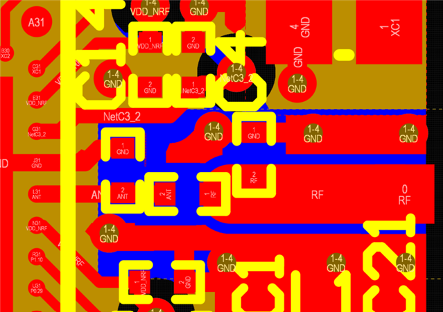
In (1) and (2) all copper on the the inner layers underneath the matching netork at the nRF5340 ANT pin is removed. The copper polygon on the bottom layer is the reference plane for both the matching network and the transmission line going to the antenna. 

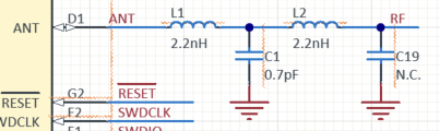
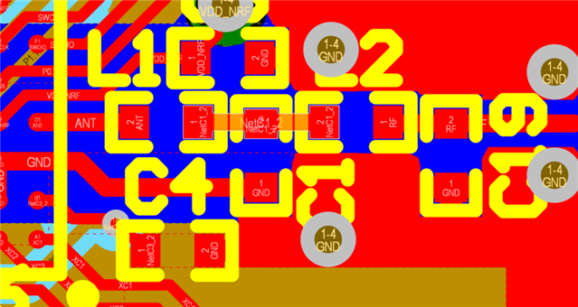
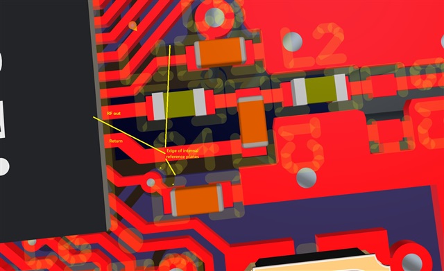
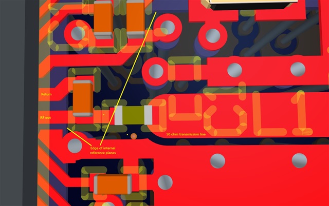
On (3), copper on inner layer 1, the one just below the micro, acts as reference plane for the capacitor closest to the ANT pin and the first terminal of the series inductor. The transmission line between the matching network and the antenna is referenced to another copper plane further down. 

Matching network ground references

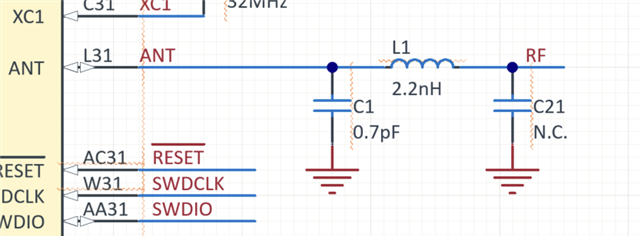
(1) and (2) First matching capacitor connected directly to GND pin on the micro, not to ground copper pour. This is in line with the recommendations in the datasheet

(3) First matching capacitor connected directly to GND pin on the micro AND to ground reference plane on inner layer 1.
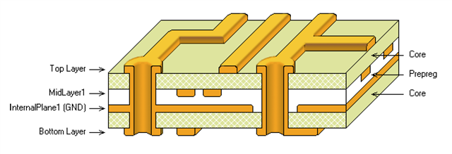
Board configuration

The board that I work on now has 7 layers in a symmetric stackup with 3+1+3 copper layers. The 3 layer stacks are connected with micro vias and the single layer in the center is a flex layer. The intention for the radio section is to use the flex layer as reference plane to achieve copper traces with similar width as the matching components for the radio. The center GND balls of the BGA package will have through hole vias to connect 0V on all layers. 

Question

Which reference plane should the matching network between the microcontroller and the 50 ohm transmission line use? The same, as for (1) and (2), or split between the different sides of the matching network, as (3)?

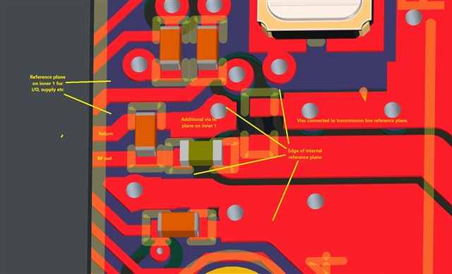
nRF5340 Audio DK (3)

nrf5340_claa_config2 (1)

nRF5340 DK (2)

Parents
  • QFN and CSP versions have different configuration.

    QFN uses two components

    Note how the first cap is only grounded via the center pad and the VSS pin only

    CSP uses three components:

    The shunt cap here is also connected to the VSS pin only.

    The inner ground planes are cut under the matching network components to reduce parasitic capacitance. There must be a ground plane under the matching network on at least one layer. If the bottom layer is not ground, the second to last layer can be used as ground plane.

  • I am aware of the differences between the QFN and BGA packages and our design uses the BGA. However, as the documentation was not totally clear in a couple of points, so I decided to have a look at the demo boards and reference layouts for guidance. As the nRF5340 Audio DK board is newer than the nRF5340 DK board, you would assume that corrective actions from known issues would be included on that, but instead the reported differences will raise more questions. The Altium files for the Audio DK also includes impedance definitions in the layer stack, which the other board don't have, so again the first impression is that this board would be better to use as a guideline.

    Based on the answers it seems that the layout on the nRF5340 Audio DK is not following the recommendations given in your reply.

    - The shunt capacitor has an additional GND via outside of the capacitor instead of just routing it back to the VSS pin (C2 on the BGA).
    -  The ground reference plane underneath the matching network is not cut in the same way as underneath the transmission line.

    When it comes to the ground reference plane, wouldn't it make more sense to have a clear definition of this in the datasheet and/or appnote? On the nRF5340 Audio DK, different copper layers are used as reference plane on each side of the matching network. Wouldn't it make more sense to keep all of the RF related signals referenced to the same reference plane? On the nRF5340 Audio DK it would also have the benefit of reduced parasitic capacitive coupling for the matching network with additional cutout on the first 2 inner layers.

  • The latest DKs files are always the reference.

    When it comes to impedance control, it only matters of you have a transmission line. The matching network have the impedance between the components all over the place so no need for impedance control here.

    NiklasNNL said:
    Wouldn't it make more sense to keep all of the RF related signals referenced to the same reference plane?

    Yes, indeed. Some layer need to carry the return current.

Reply
  • The latest DKs files are always the reference.

    When it comes to impedance control, it only matters of you have a transmission line. The matching network have the impedance between the components all over the place so no need for impedance control here.

    NiklasNNL said:
    Wouldn't it make more sense to keep all of the RF related signals referenced to the same reference plane?

    Yes, indeed. Some layer need to carry the return current.

Children
No Data
Related