Problems with nRF9151 - cannot connect over SWD - higher current consumption

Hello,

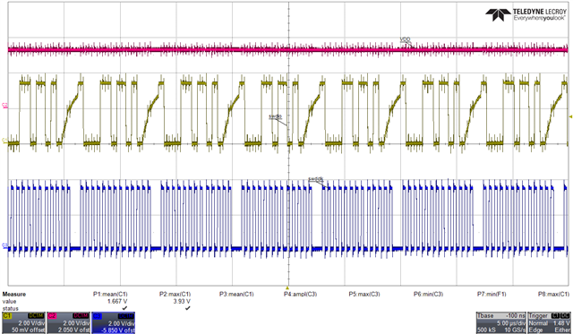
we have produced 10 Boards with nRF9151. Unfortunately, 3 device shows a false behavior. We cannot connect over SWD an they have a larger power consumption (whole circuit) of 24mA instead of 5mA in case of the good one (measured without firmware). 

Also nReset is permanently low without connection though other components in the circuit. VDD has 3.3V but error message says "Low voltage 0"

Component NRF9151 reacts to external heat and external cold temperature in form of other error messages. 

Do you have an idea ? 

Error Messages: 

1:

[error] [ Client] - Encountered error -12: Command connect_to_emu_with_snr executed for 111 milliseconds with result -12
164210439  - UNKNOWN
[error] [ Worker] - Low voltage 0 detected in target device.

2:

[error] [ Client] - Encountered error -102: Command connect_to_emu_with_snr executed for 173 milliseconds with result -102
164210439  - UNKNOWN
[error] [ Worker] - An unknown error.

3: 

08:51:25.871

Failed "reading readback protection status for application core". Error: code: 1, description: Generic, message: Batch task protection-get failed, [Probe] Device error: Failed to configure Coresight: LOW_VOLTAGE

08:51:25.997

Error: Failed with exit code 1. One or more batch tasks failed: - [Probe] Device error: Failed to configure Coresight: LOW_VOLTAGE, code: Generic. Message: Batch task protection-get failed, [Probe] Device error: Failed to configure Coresight: LOW_VOLTAGE.

10:17:38.426

Error: Failed with exit code 1. Failed to device info one or more devices: * 164210439: [Probe] Device error: Failed to write DebugPort register 2: Unknown Error in J-Link DLL (error code =-1), code: Generic. Message: Operation device-info failed, [Probe] Device error: Failed to write DebugPort register 2: Unknown Error in J-Link DLL (error code =-1).

  • Hello Walerijm
    the situation you describe sounds like there's one or more shorts between pins/pads on the nRF9151 package on your PCB. I assume the numbers you are using (1-3) referes to the units with faults?
    1: This error message we often see when the device to be programmed doesn't have the right voltage or that the reference on the SWD/JTAG interface isn't there. You have checked VDD all around this unit and they are all as epxtected? What about the VDD_REF on the JTAG, is that the level that you expect? 
    2: This could be many issues again, the VDD is first thing to check, is it as expected on all? If VDD is stable and at the right level, could you check the SWD interface compared to GND to see if you might have a short betweeon one of them and GND?
    3: Which commands are you using here? Which tools are you using to program it? Once again, the low voltage claim makes me initially want to check the VDD and SWD pins. 
    I'm sorry not to be able to give you a better answer, but the errors you see matches the behaviour of units where there are shorts between some functional pin(s) and GND. Have you looked at the boards in microscope? Hows the assembly looking, any shorts that you can see around the edged of the package? 
    Best regards
    Asbjørn
  • Hi, thanks for the answer. The number I am using are different tries to connect via SWD. The affected units behave very similar.

    1.  VDD and VDD_GPIO is fine at 3.3V. Also VDD_Ref on JTAG.

    2.  There is no short within or between SWD and GND.

    3. We sent the unit to a X-Ray investigation. The result is a lack of solder or porous soldering on several pins. These include several GND pins as well as Pin 14 (VDD). Can this behavior be explainable through bad soldered units?

  • Hello Walerij,
    The low power warning is confusing in all of this. That is the warning when the reference voltage is not there or lower than 3.3V. But you say you measure 3.3V on VDD; VDD_GPIO and VDD_Ref. The SWDIO and SWDCLK pins are they toggling as expected? Are you able to capture with an oscilloscope?
    Q2: See above, are the pins toggling as expected and same as on the failing devices as on the functional ones?
    Q3: Bad soldering could explain this, absolutely, that's why I'm curious if there's actually signal toggling on the SWDIO/SWDCLK pins? Are the lack of solder and porous occuring on the same pins or same area of the SIP? Are the ones with pin14 (VDD) the ones that gives the error message of low voltage? Are they also showing VDD=3.3V?
    Best regards
    Asbjørn
  • Hi, VDD=3.3V should be fine. SWDIO and SWDCLK are toggling. I am wondering why my current consumption is higher than in "normal" mode. 

    Normal Mode (when programming is posible)= 5mA

    Problem mode (when programming is not possible) = 25mA.

    Error Code: 

    16:49:59.247
    Failed "reading readback protection status for application core". Error: code: 1, description: Generic, message: Batch task protection-get failed, Device error: Setting the debug port SELECT register failed while powering up sys and debug regions (Unknown Error in J-Link DLL (error code =-2)). This might indicate that the debug port is unavailable. Please double-check device power supply and SWD lines, and that SWD isn't disabled
    16:49:59.259
    Error: Failed with exit code 1. One or more batch tasks failed: * 811003700: Device error: Setting the debug port SELECT register failed while powering up sys and debug regions (Unknown Error in J-Link DLL (error code =-2)). This might indicate that the debug port is unavailable. Please double-check device power supply and SWD lines, and that SWD isn't disabled (Generic) Message: Batch task protection-get failed, Device error: Setting the debug port SELECT register failed while powering up sys and debug regions (Unknown Error in J-Link DLL (error code =-2)). This might indicate that the debug port is unavailable. Please double-check device power supply and SWD lines, and that SWD isn't disabled.
    Next week I am going to test a new batch of hardware. In this design there should be solved the lack of solder. We considered the new hardware design guide with new solder paste stencil and improved footprint... 
  • Hello Walerij,
    This difference in current consumption makes me still think there's some short somewhere on the board. You measure 5ma on the board you can program. In which states are they when you measure 5mA? Is that before you try to program them?
    Could you check to see if any of the other VDD/power supply/decoupling  on this boards might be shorted to GND somehow?
    Did the xray investigation show any signs of shorts somewhere on under the SiP?
    Did you receive the new batch of board, how did they perform and what specifically did you alter between the builds?
    Best regards
    Asbjørn
Related