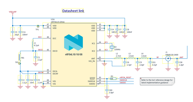
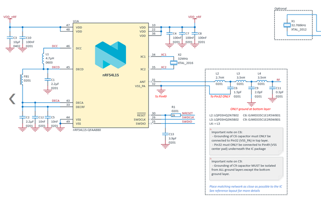
For VDD-nRF in the nRF54L15-DK schematic
When I check the schematic, I can't tell which part is internally generated.
When I check the actual board, VDDM_nRF and VDD_nRF are separated, but
Is it correct to interpret that the voltage input to 48Pin of nRF54L15-QFAABB0 is supplied to 47Pin section via inside of nRF54L15-QFAABB0?