Hello!
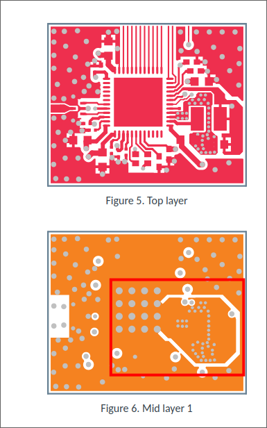
I am working to design and build a custom PCB using the nRF7002 chip and came across this callout on the schematic diagram and wanted some clarification about it. The PCB that I am working on is using a much more compact form factor than the reference diagram suggests so I would like to make sure any adaptation made with the custom board allows for full functionality of the chip.
1) Is there a distinct purpose to the solid metal plane in this suggested circuit?
2)What is the effect on the functionality if it is changed?
3) If this component is used on a board with the nRF5340 or a similar device, will the entire panel require the solid plane or just the section under the nRF7002?
Thank You.


