Matching Antenna to the nRF52832

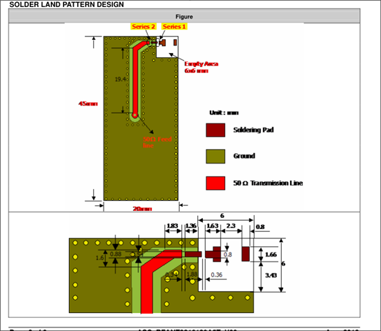
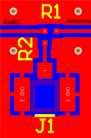
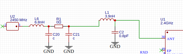
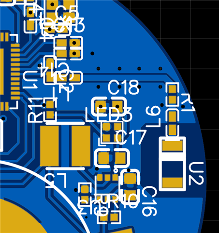
Previously, I designed a PCB for the nRF52832 chip using the RFANT3216120A5T antenna (link). However, I was only able to achieve a very limited Bluetooth range of around 6 meters. The design details are as follows.

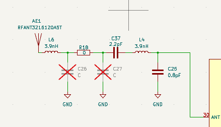
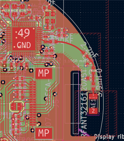
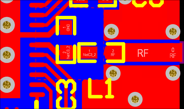
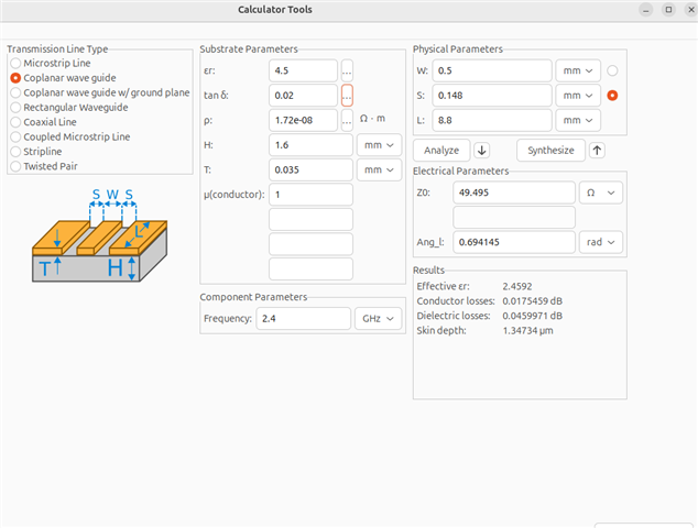
In the previous version, I identified some mistakes related to trace width calculations and RF routing. I have redesigned the circuit considering these issues and updated the parameters accordingly. Before placing an order for the new PCB, I would like to confirm whether this revised design is correct and whether it can achieve a Bluetooth range of up to 30 meters.

Please note that I do not have access to antenna tuning equipment.

Parents
  • Hi,

    Could you clarify, which is the new version of the PCB?

    The antenna datasheet show that this antenna must be mounted in the corner of a rectangular PCB:

    The antenna won't be radiating correctly when there is GND in "front" of it:


    Best regards,

    Bendik

  • Hi,

    The secondly mentioned blue color one is the new version.

    It menas i cant use the round shape for my pcb no?

    Ok i will correct the gnd plane.

    I also add the sma connector to the rf path.


    Thank you,
    Anjula

  • Anjula said:
    The secondly mentioned blue color one is the new version.

    Thanks for confirming.

    There are a couple of components missing from the antenna matching network in this version of the board. The two shunt capacitors must be added back to the antenna matching network. These capacitors could be needed when tuning the antenna, so there must be a footprint available for them.

    C2 must be grounded to only the VSS pin 31 and the center GND pad, and not to the top layer GND fill. This is done to improve the attenuation of the second harmonic frequency. Here is a snippet from the reference layout showing the correct grounding of this capacitor:

    Anjula said:
    It menas i cant use the round shape for my pcb no?

    It could be OK, but chip antennas usually have a minimum ground plane size needed for optimal operation. The antenna datasheet does not mention a minium size so it may be OK to use it on a smaler board, with the modifications to the GND plane.

    Anjula said:
    I also add the sma connector to the rf path.

    We don't recommend adding a non switching RF connector directly to the RF path.

    For this type of connector it is best to connect it to the RF path using 0 Ohm links, so that it can be isolated for the RF path when not in use. If both the RF connector and the on board antenna is connected at the same time, there will be some loss of power resulting in incorrect measurements from the RF connector.
    Here is way to add a RF connector to the RF path without creating RF stubs using two 0 Ohm links sharing one pad:

    In this setup only R1 or R2 are populated at a time.

Reply
  • Anjula said:
    The secondly mentioned blue color one is the new version.

    Thanks for confirming.

    There are a couple of components missing from the antenna matching network in this version of the board. The two shunt capacitors must be added back to the antenna matching network. These capacitors could be needed when tuning the antenna, so there must be a footprint available for them.

    C2 must be grounded to only the VSS pin 31 and the center GND pad, and not to the top layer GND fill. This is done to improve the attenuation of the second harmonic frequency. Here is a snippet from the reference layout showing the correct grounding of this capacitor:

    Anjula said:
    It menas i cant use the round shape for my pcb no?

    It could be OK, but chip antennas usually have a minimum ground plane size needed for optimal operation. The antenna datasheet does not mention a minium size so it may be OK to use it on a smaler board, with the modifications to the GND plane.

    Anjula said:
    I also add the sma connector to the rf path.

    We don't recommend adding a non switching RF connector directly to the RF path.

    For this type of connector it is best to connect it to the RF path using 0 Ohm links, so that it can be isolated for the RF path when not in use. If both the RF connector and the on board antenna is connected at the same time, there will be some loss of power resulting in incorrect measurements from the RF connector.
    Here is way to add a RF connector to the RF path without creating RF stubs using two 0 Ohm links sharing one pad:

    In this setup only R1 or R2 are populated at a time.

Children
No Data
Related