MISO line mimics the MOSI line in SPIM configuration sdk 17.1.0

Hi,

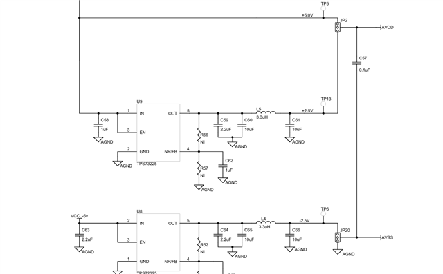
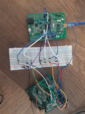
When I looked at the SPI lines using the oscilloscope, I saw that the MISO line had the same signal as the MOSI line. As you can see from the image, basically SPI configuration works properly. Before message transfer CS pin goes low, and after that, the MOSI line works. I can read message that I sent using the oscilloscope.

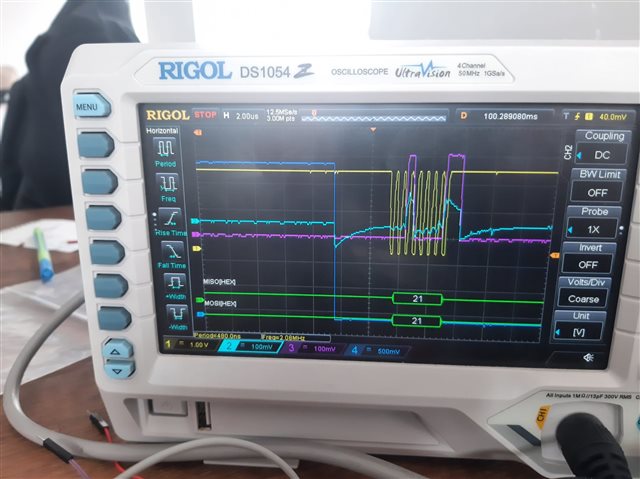
What can be the problem with the MISO line signal reflecting the MOSI line signal? The SPI config stage CPOL = 0, CPAH = 1, I am using a 2 MHz clock signal. Thanks for your help.

Parents
  • Schematic. Looks to me like MISO was never driven at all and is just floating. The voltage change results from coupling to MOSI and clock signal.

    MISO is supposed to be driven by the slave when CS=Low. Check that its properly connected. 

  • Sorry for the late response. All physical pins are connected properly, but I did not understand the problem. During the SPIM configuration, I just initialised the MISO pin. I am sharing my ADS1299 library code with you, Maybe the issue is about the software configuration of the SPIM. I checked the working mechanism of the SPI with ADS1299, and it looks like it was working properly. Again, thanks for your help.


    #include "ADS1299_nRF.h"
    #include <nrf.h>
    #include <nrf_log.h>
    #include <nrf_log_ctrl.h>
    #include <nrf_log_default_backends.h>
    #include <nrf_gpio.h>
    #include <nrf_delay.h>
    #include "ads1299_delay.h"
    
    // Enable polling mode for DRDY
    #define POLL_DREADY
    
    #define SPIM2 NRF_SPIM2
    
    bool new_data_available = false;
    uint8_t rx_buffer[27], tx_buffer[8];
    uint8_t sample_number = 0;
    static uint8_t regData[24]; // Mirror of ADS1299 registers
    
    
    /** @brief SPI interface initialization. Accurate timing use HFCLK clock */
    void spi_init(void) {
        // Start HFCLK source for accurate timing
        NRF_CLOCK->TASKS_HFCLKSTART = 1;
        while (NRF_CLOCK->EVENTS_HFCLKSTARTED == 0);
        NRF_CLOCK->EVENTS_HFCLKSTARTED = 0;
        
        // Disable SPIM to configure it
        SPIM2->ENABLE = (SPIM_ENABLE_ENABLE_Disabled << SPIM_ENABLE_ENABLE_Pos);
    
        // Configure SPIM2 pins
        SPIM2->PSEL.SCK = PIN_SCK;
        SPIM2->PSEL.MOSI = PIN_MOSI;
        SPIM2->PSEL.MISO = PIN_MISO;
        
        SPIM2->FREQUENCY = SPIM_FREQUENCY_FREQUENCY_M2; // 2 MHz
    
        // ADS1299 set Data mode clock polarity = 0; clock_phase = 1
        SPIM2->CONFIG = (SPIM_CONFIG_CPOL_ActiveLow << SPIM_CONFIG_CPOL_Pos) |  // Fixed CPOL
                        (SPIM_CONFIG_CPHA_Trailing << SPIM_CONFIG_CPHA_Pos) |
                        (SPIM_CONFIG_ORDER_MsbFirst << SPIM_CONFIG_ORDER_Pos);
    
        SPIM2->EVENTS_END = 0;
        SPIM2->EVENTS_ENDTX = 0;
        SPIM2->EVENTS_ENDRX = 0;
        SPIM2->EVENTS_STOPPED = 0;
    
        SPIM2->ENABLE = (SPIM_ENABLE_ENABLE_Enabled << SPIM_ENABLE_ENABLE_Pos);
        
    }
    
    static void spi_uninit(void) {
        SPIM2->ENABLE = (SPIM_ENABLE_ENABLE_Disabled << SPIM_ENABLE_ENABLE_Pos);
        nrf_gpio_cfg_input(PIN_SCK, NRF_GPIO_PIN_NOPULL);
        nrf_gpio_cfg_input(PIN_MOSI, NRF_GPIO_PIN_NOPULL);
        nrf_gpio_cfg_input(PIN_MISO, NRF_GPIO_PIN_NOPULL);
    }
    
    //bool spi_transfer_byte(uint8_t tx, uint8_t *rx) {
    //    uint8_t local_rx = 0;
    //    if (!rx) rx = &local_rx;
    //    if (!(SPIM2->ENABLE & SPIM_ENABLE_ENABLE_Msk)) {
    //        SPIM2->ENABLE = (SPIM_ENABLE_ENABLE_Enabled << SPIM_ENABLE_ENABLE_Pos);
    //    }
    //    SPIM2->TXD.PTR = (uint32_t)&tx;
    //    SPIM2->TXD.MAXCNT = 1;
    //    SPIM2->RXD.PTR = (uint32_t)rx;
    //    SPIM2->RXD.MAXCNT = 1;
    //    SPIM2->EVENTS_END = 0;
    //    SPIM2->TASKS_START = 1;
    
    //    nrf_delay_us(20);
    
    //    //uint32_t timeout = 10000;
    //    //while (!SPIM2->EVENTS_END && timeout--) {
    //    //    nrf_delay_us(1);
    //    //}
    //    //if (timeout == 0) {
    //    //    NRF_LOG_ERROR("SPI transfer timeout");
    //    //    return false;
    //    //}
    //    SPIM2->EVENTS_END = 0;
    //    NRF_LOG_INFO("SPI TX: 0x%02x, RX: 0x%02x", tx, *rx);
    //    return true;
    //}
    
    uint8_t spi_transfer_byte(uint8_t tx) {
        uint8_t rx;
        if (!(SPIM2->ENABLE & SPIM_ENABLE_ENABLE_Msk)) {
            SPIM2->ENABLE = (SPIM_ENABLE_ENABLE_Enabled << SPIM_ENABLE_ENABLE_Pos);
        }
        SPIM2->TXD.PTR = (uint32_t)&tx;
        SPIM2->TXD.MAXCNT = 1;
        SPIM2->RXD.PTR = (uint32_t)&rx;
        SPIM2->RXD.MAXCNT = 1;
        SPIM2->EVENTS_END = 0;
        SPIM2->TASKS_START = 1;
        while (!SPIM2->EVENTS_END);
        SPIM2->EVENTS_END = 0;
        //SPIM2->TASKS_STOP = 1;
        NRF_LOG_INFO("SPI TX: 0x%02x, RX: 0x%02x", tx, rx);
        return rx;
    }
    
    bool spi_transfer_byte_v2(uint8_t tx, uint8_t *rx) {
        uint8_t local_rx = 0;
        if (!rx) rx = &local_rx;
        
        // Ensure SPIM2 is enabled (assumes prior configuration)
        if (!(SPIM2->ENABLE & SPIM_ENABLE_ENABLE_Msk)) {
            SPIM2->ENABLE = (SPIM_ENABLE_ENABLE_Enabled << SPIM_ENABLE_ENABLE_Pos);
        }
        
        // Clear events before starting
        SPIM2->EVENTS_ENDTX = 0;
        SPIM2->EVENTS_ENDRX = 0;
        SPIM2->EVENTS_END = 0;
        
        // Configure buffers
        SPIM2->TXD.PTR = (uint32_t)&tx;
        SPIM2->TXD.MAXCNT = 1;
        SPIM2->RXD.PTR = (uint32_t)rx;
        SPIM2->RXD.MAXCNT = 1;
        
        // Start transaction
        SPIM2->TASKS_START = 1;
        
        // Wait for transaction to complete
        while (!SPIM2->EVENTS_END);
        
        // Clear events
        SPIM2->EVENTS_ENDTX = 0;
        SPIM2->EVENTS_ENDRX = 0;
        SPIM2->EVENTS_END = 0;
    
        NRF_LOG_INFO("SPI TX: 0x%02x, RX: 0x%02x", tx, *rx);
        return true;
    }
    
    bool ADS1299_init(void) {
        
        // recommended power up sequence for ADS1299
        delay_init();
        nrf_delay_ms(50);
        
        NRF_LOG_INFO("Initializing ADS1299");
        nrf_gpio_pin_clear(RESET_PIN);
        nrf_gpio_cfg_output(RESET_PIN);
        nrf_gpio_pin_clear(RESET_PIN);
        nrf_delay_us(4);
        nrf_gpio_pin_set(RESET_PIN);
        nrf_delay_us(20);
        
        //nrf_gpio_cfg_output(PIN_SCK);
        //nrf_gpio_cfg_output(PIN_MOSI);
        
        //nrf_gpio_pin_clear(PIN_SCK);
        //nrf_gpio_pin_clear(PIN_MOSI);
        
        spi_init();
    
        nrf_gpio_cfg_input(PIN_DRDY,NRF_GPIO_PIN_NOPULL);
    
        nrf_gpio_pin_set(CS_PIN);
        //NRF_GPIO->PIN_CNF[CS_PIN] = (GPIO_PIN_CNF_DIR_Output << GPIO_PIN_CNF_DIR_Pos) |
        //                            (GPIO_PIN_CNF_DRIVE_S0S1 << GPIO_PIN_CNF_DRIVE_Pos) |
        //                            (GPIO_PIN_CNF_INPUT_Connect << GPIO_PIN_CNF_INPUT_Pos) |
        //                            (GPIO_PIN_CNF_PULL_Disabled << GPIO_PIN_CNF_PULL_Pos) |
        //                            (GPIO_PIN_CNF_SENSE_Disabled << GPIO_PIN_CNF_SENSE_Pos);
    
        nrf_gpio_cfg_output(CS_PIN);
    
        nrf_gpio_pin_set(CS_PIN);
        nrf_gpio_pin_set(RESET_PIN);
    
        NRF_LOG_INFO("SPI init success");
    #ifdef POLL_DREADY
        NRF_LOG_INFO("DRDY polling enabled");
    #else
        NRF_LOG_INFO("DRDY interrupt not implemented");
    #endif
        return true;
    }
    
    void poll_dready(void) {
    #ifdef POLL_DREADY
        NRF_LOG_INFO("Polling DRDY, state: %d", nrf_gpio_pin_read(PIN_DRDY));
        if (nrf_gpio_pin_read(PIN_DRDY) == 0) {
            NRF_LOG_INFO("DRDY low, receiving data");
            ADS1299_receive_data();
            send_new_available_data();
        }
    #endif
    }
    
    bool ADS1299_write_register(uint8_t address, uint8_t value) {
    
        uint8_t opcode1 = address | COMMAND_WREG;
        nrf_gpio_pin_clear(CS_PIN);
    
        //if (!spi_transfer_byte_v2(opcode1, NULL)) {
        //    nrf_gpio_pin_set(CS_PIN);
        //    return false;
        //}
        //if (!spi_transfer_byte_v2(0x00, NULL)) {
        //    nrf_gpio_pin_set(CS_PIN);
        //    return false;
        //}
        //if (!spi_transfer_byte_v2(value, NULL)) {
        //    nrf_gpio_pin_set(CS_PIN);
        //    return false;
        //}
        
        spi_transfer_byte(opcode1);
        spi_transfer_byte(0x00);
        spi_transfer_byte(value);
        nrf_delay_us(4);
        nrf_gpio_pin_set(CS_PIN);
        regData[address] = value;
        
        
        return true;
    }
    
    bool ADS1299_read_register(uint8_t address, uint8_t *value) {
        uint8_t opcode1 = address | COMMAND_RREG;
        
        nrf_gpio_pin_clear(CS_PIN);
    
        //if (!spi_transfer_byte_v2(opcode1, NULL)) {
        //    nrf_gpio_pin_set(CS_PIN);
        //    return false;
        //}
        //if (!spi_transfer_byte_v2(0x00, NULL)) {
        //    nrf_gpio_pin_set(CS_PIN);
        //    return false;
        //}
        //if (!spi_transfer_byte_v2(0x00, value)) {
        //    nrf_gpio_pin_set(CS_PIN);
        //    return false;
        //}
        
        spi_transfer_byte(opcode1);
        spi_transfer_byte(0x00);
        *value = spi_transfer_byte(0x00);
    
        nrf_delay_us(4);
    
        nrf_gpio_pin_set(CS_PIN);
    
        regData[address] = *value;
        
        return true;
    }
    
    bool ADS1299_send_command(uint8_t command) {
        uint8_t dummy;
        nrf_gpio_pin_clear(CS_PIN);
        //if (!spi_transfer_byte_v2(command, &dummy)) {
        //    NRF_LOG_ERROR("Failed to send command 0x%02x", command);
        //    nrf_gpio_pin_set(CS_PIN);
        //    return false;
        //}
        spi_transfer_byte(command);
    
        nrf_delay_us(4);
        nrf_gpio_pin_set(CS_PIN);
        return true;
    }
    
    bool ADS1299_send_start(void) {
    
        bool result = ADS1299_send_command(COMMAND_START);    
        return result;
    }
    
    bool ADS1299_send_read_continuous(void) {
        bool result = ADS1299_send_command(COMMAND_RDATAC);
        nrf_delay_us(3);
        return result;
    }
    
    bool ADS1299_send_reset(void) {
        //nrf_gpio_pin_clear(CS_PIN);
        bool result = ADS1299_send_command(COMMAND_RESET);
        nrf_delay_us(20);
        //nrf_gpio_pin_set(CS_PIN);
        NRF_LOG_INFO("Reset command sent, result: %d", result);
        return result;
    }
    
    bool ADS1299_send_sdatac(void) {
        //nrf_gpio_pin_clear(CS_PIN);
        bool result = ADS1299_send_command(COMMAND_SDATAC);
        //nrf_gpio_pin_set(CS_PIN);
        nrf_delay_ms(10);
        NRF_LOG_INFO("Stop read continuously command sent, result: %d", result);
        return result;
    }
    
    bool ADS1299_receive_data(void) {
        new_data_available = false;
        if (!spi_transfer_bytes(NULL, rx_buffer, 27)) {
            NRF_LOG_ERROR("Failed to receive data");
            return false;
        }
        new_data_available = true;
        NRF_LOG_INFO("Data received, triggering send_new_available_data");
        return true;
    }
    
    bool ADS1299_poll_new_data(ADS1299_data_t *data) {
        if (new_data_available) {
            new_data_available = false;
            *data = ADS1299_convert_data();
            return true;
        }
        return false;
    }
    
    static inline int32_t buffer_to_channel(uint8_t id) {
        int32_t value = (rx_buffer[3 + id * 3] << 16) | (rx_buffer[4 + id * 3] << 8) | rx_buffer[5 + id * 3];
        if (value & 0x00800000) {
            value |= 0xFF000000;
        } else {
            value &= 0x00FFFFFF;
        }
        return value;
    }
    
    ADS1299_data_t ADS1299_convert_data(void) {
        ADS1299_data_t data;
        data.lead_off_positive = rx_buffer[0] << 4;
        data.lead_off_positive |= (rx_buffer[1] & 0b11110000) >> 4;
        data.lead_off_negative = rx_buffer[1] << 4;
        data.lead_off_negative |= (rx_buffer[2] & 0b11110000) >> 4;
        data.gpio_0 = rx_buffer[2] & 0b00001000;
        data.gpio_1 = rx_buffer[2] & 0b00000100;
        data.gpio_2 = rx_buffer[2] & 0b00000010;
        data.gpio_3 = rx_buffer[2] & 0b00000001;
        data.channel_0 = buffer_to_channel(0);
        data.channel_1 = buffer_to_channel(1);
        data.channel_2 = buffer_to_channel(2);
        data.channel_3 = buffer_to_channel(3);
        data.channel_4 = buffer_to_channel(4);
        data.channel_5 = buffer_to_channel(5);
        data.channel_6 = buffer_to_channel(6);
        data.channel_7 = buffer_to_channel(7);
        return data;
    }
    
    void send_new_available_data(void) {
        if (new_data_available) {
            new_data_available = false;
            NRF_LOG_INFO("Sample: %d", sample_number++);
            for (uint8_t i = 0; i < 27; i++) {
                NRF_LOG_INFO("Byte %d: 0x%02x", i, rx_buffer[i]);
            }
        }
    }

  •   I could not find the DVSS pin. AVSS present, but there is no DVSS pin in the datasheet. 

  • DVDD and AVDD are connected to the 3V of the STM32.

    Wait, that is illegal on the ADS1299. You can do so only on the ADS1298(R), as it can use the 2.5V reference.

    The ADS1299 specs a 4.5V reference that requires symmetric +-2.5V for AVDD/AVSS. These voltages should be generated on the test board in your pictures.

    I am not sure what the supply rails are called on the test board schematic, but you should measure 5V between AVDD and AVSS going into the ADS chip.

    You can connect +3.3V to the test board supply rails but not directly to the analog input rails for the ADS chip. Connecting 3.3V directly here may damage the chip.

  • Should I adhere to this rule when creating the ADS1299 PCB? Because I will create the ADS1299 PCB with the nRF52 in the next stage of my development. 

    Note:
    When I power up ADS1299, I can see VCAP1 over 1.1V after 30s, and it goes, and I can't read or write again to the register. Probably the problem is the power supply method of the board. The nRF side is again useless, I can't communicate with ADS1299 at all.

  • "It would help if you can list in detail all the connections to the board, in particular J4 but all the settings would be useful, both jumper settings and external supplies"

    I know it is tedious, but unless you post every connection to the ADS1299 board and the jumper settings on the board we will not be able to establish if they are correct.

Reply Children
Related