MISO line mimics the MOSI line in SPIM configuration sdk 17.1.0

Hi,

When I looked at the SPI lines using the oscilloscope, I saw that the MISO line had the same signal as the MOSI line. As you can see from the image, basically SPI configuration works properly. Before message transfer CS pin goes low, and after that, the MOSI line works. I can read message that I sent using the oscilloscope.
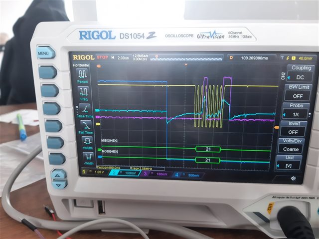
What can be the problem with the MISO line signal reflecting the MOSI line signal? The SPI config stage CPOL = 0, CPAH = 1, I am using a 2 MHz clock signal. Thanks for your help.

Parents
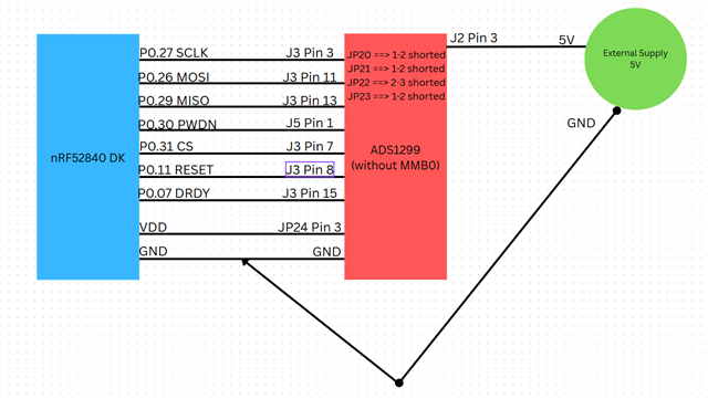
  • Schematic. Looks to me like MISO was never driven at all and is just floating. The voltage change results from coupling to MOSI and clock signal.

    MISO is supposed to be driven by the slave when CS=Low. Check that its properly connected. 

  • Sorry for the late response. All physical pins are connected properly, but I did not understand the problem. During the SPIM configuration, I just initialised the MISO pin. I am sharing my ADS1299 library code with you, Maybe the issue is about the software configuration of the SPIM. I checked the working mechanism of the SPI with ADS1299, and it looks like it was working properly. Again, thanks for your help.


    #include "ADS1299_nRF.h"
    #include <nrf.h>
    #include <nrf_log.h>
    #include <nrf_log_ctrl.h>
    #include <nrf_log_default_backends.h>
    #include <nrf_gpio.h>
    #include <nrf_delay.h>
    #include "ads1299_delay.h"
    
    // Enable polling mode for DRDY
    #define POLL_DREADY
    
    #define SPIM2 NRF_SPIM2
    
    bool new_data_available = false;
    uint8_t rx_buffer[27], tx_buffer[8];
    uint8_t sample_number = 0;
    static uint8_t regData[24]; // Mirror of ADS1299 registers
    
    
    /** @brief SPI interface initialization. Accurate timing use HFCLK clock */
    void spi_init(void) {
        // Start HFCLK source for accurate timing
        NRF_CLOCK->TASKS_HFCLKSTART = 1;
        while (NRF_CLOCK->EVENTS_HFCLKSTARTED == 0);
        NRF_CLOCK->EVENTS_HFCLKSTARTED = 0;
        
        // Disable SPIM to configure it
        SPIM2->ENABLE = (SPIM_ENABLE_ENABLE_Disabled << SPIM_ENABLE_ENABLE_Pos);
    
        // Configure SPIM2 pins
        SPIM2->PSEL.SCK = PIN_SCK;
        SPIM2->PSEL.MOSI = PIN_MOSI;
        SPIM2->PSEL.MISO = PIN_MISO;
        
        SPIM2->FREQUENCY = SPIM_FREQUENCY_FREQUENCY_M2; // 2 MHz
    
        // ADS1299 set Data mode clock polarity = 0; clock_phase = 1
        SPIM2->CONFIG = (SPIM_CONFIG_CPOL_ActiveLow << SPIM_CONFIG_CPOL_Pos) |  // Fixed CPOL
                        (SPIM_CONFIG_CPHA_Trailing << SPIM_CONFIG_CPHA_Pos) |
                        (SPIM_CONFIG_ORDER_MsbFirst << SPIM_CONFIG_ORDER_Pos);
    
        SPIM2->EVENTS_END = 0;
        SPIM2->EVENTS_ENDTX = 0;
        SPIM2->EVENTS_ENDRX = 0;
        SPIM2->EVENTS_STOPPED = 0;
    
        SPIM2->ENABLE = (SPIM_ENABLE_ENABLE_Enabled << SPIM_ENABLE_ENABLE_Pos);
        
    }
    
    static void spi_uninit(void) {
        SPIM2->ENABLE = (SPIM_ENABLE_ENABLE_Disabled << SPIM_ENABLE_ENABLE_Pos);
        nrf_gpio_cfg_input(PIN_SCK, NRF_GPIO_PIN_NOPULL);
        nrf_gpio_cfg_input(PIN_MOSI, NRF_GPIO_PIN_NOPULL);
        nrf_gpio_cfg_input(PIN_MISO, NRF_GPIO_PIN_NOPULL);
    }
    
    //bool spi_transfer_byte(uint8_t tx, uint8_t *rx) {
    //    uint8_t local_rx = 0;
    //    if (!rx) rx = &local_rx;
    //    if (!(SPIM2->ENABLE & SPIM_ENABLE_ENABLE_Msk)) {
    //        SPIM2->ENABLE = (SPIM_ENABLE_ENABLE_Enabled << SPIM_ENABLE_ENABLE_Pos);
    //    }
    //    SPIM2->TXD.PTR = (uint32_t)&tx;
    //    SPIM2->TXD.MAXCNT = 1;
    //    SPIM2->RXD.PTR = (uint32_t)rx;
    //    SPIM2->RXD.MAXCNT = 1;
    //    SPIM2->EVENTS_END = 0;
    //    SPIM2->TASKS_START = 1;
    
    //    nrf_delay_us(20);
    
    //    //uint32_t timeout = 10000;
    //    //while (!SPIM2->EVENTS_END && timeout--) {
    //    //    nrf_delay_us(1);
    //    //}
    //    //if (timeout == 0) {
    //    //    NRF_LOG_ERROR("SPI transfer timeout");
    //    //    return false;
    //    //}
    //    SPIM2->EVENTS_END = 0;
    //    NRF_LOG_INFO("SPI TX: 0x%02x, RX: 0x%02x", tx, *rx);
    //    return true;
    //}
    
    uint8_t spi_transfer_byte(uint8_t tx) {
        uint8_t rx;
        if (!(SPIM2->ENABLE & SPIM_ENABLE_ENABLE_Msk)) {
            SPIM2->ENABLE = (SPIM_ENABLE_ENABLE_Enabled << SPIM_ENABLE_ENABLE_Pos);
        }
        SPIM2->TXD.PTR = (uint32_t)&tx;
        SPIM2->TXD.MAXCNT = 1;
        SPIM2->RXD.PTR = (uint32_t)&rx;
        SPIM2->RXD.MAXCNT = 1;
        SPIM2->EVENTS_END = 0;
        SPIM2->TASKS_START = 1;
        while (!SPIM2->EVENTS_END);
        SPIM2->EVENTS_END = 0;
        //SPIM2->TASKS_STOP = 1;
        NRF_LOG_INFO("SPI TX: 0x%02x, RX: 0x%02x", tx, rx);
        return rx;
    }
    
    bool spi_transfer_byte_v2(uint8_t tx, uint8_t *rx) {
        uint8_t local_rx = 0;
        if (!rx) rx = &local_rx;
        
        // Ensure SPIM2 is enabled (assumes prior configuration)
        if (!(SPIM2->ENABLE & SPIM_ENABLE_ENABLE_Msk)) {
            SPIM2->ENABLE = (SPIM_ENABLE_ENABLE_Enabled << SPIM_ENABLE_ENABLE_Pos);
        }
        
        // Clear events before starting
        SPIM2->EVENTS_ENDTX = 0;
        SPIM2->EVENTS_ENDRX = 0;
        SPIM2->EVENTS_END = 0;
        
        // Configure buffers
        SPIM2->TXD.PTR = (uint32_t)&tx;
        SPIM2->TXD.MAXCNT = 1;
        SPIM2->RXD.PTR = (uint32_t)rx;
        SPIM2->RXD.MAXCNT = 1;
        
        // Start transaction
        SPIM2->TASKS_START = 1;
        
        // Wait for transaction to complete
        while (!SPIM2->EVENTS_END);
        
        // Clear events
        SPIM2->EVENTS_ENDTX = 0;
        SPIM2->EVENTS_ENDRX = 0;
        SPIM2->EVENTS_END = 0;
    
        NRF_LOG_INFO("SPI TX: 0x%02x, RX: 0x%02x", tx, *rx);
        return true;
    }
    
    bool ADS1299_init(void) {
        
        // recommended power up sequence for ADS1299
        delay_init();
        nrf_delay_ms(50);
        
        NRF_LOG_INFO("Initializing ADS1299");
        nrf_gpio_pin_clear(RESET_PIN);
        nrf_gpio_cfg_output(RESET_PIN);
        nrf_gpio_pin_clear(RESET_PIN);
        nrf_delay_us(4);
        nrf_gpio_pin_set(RESET_PIN);
        nrf_delay_us(20);
        
        //nrf_gpio_cfg_output(PIN_SCK);
        //nrf_gpio_cfg_output(PIN_MOSI);
        
        //nrf_gpio_pin_clear(PIN_SCK);
        //nrf_gpio_pin_clear(PIN_MOSI);
        
        spi_init();
    
        nrf_gpio_cfg_input(PIN_DRDY,NRF_GPIO_PIN_NOPULL);
    
        nrf_gpio_pin_set(CS_PIN);
        //NRF_GPIO->PIN_CNF[CS_PIN] = (GPIO_PIN_CNF_DIR_Output << GPIO_PIN_CNF_DIR_Pos) |
        //                            (GPIO_PIN_CNF_DRIVE_S0S1 << GPIO_PIN_CNF_DRIVE_Pos) |
        //                            (GPIO_PIN_CNF_INPUT_Connect << GPIO_PIN_CNF_INPUT_Pos) |
        //                            (GPIO_PIN_CNF_PULL_Disabled << GPIO_PIN_CNF_PULL_Pos) |
        //                            (GPIO_PIN_CNF_SENSE_Disabled << GPIO_PIN_CNF_SENSE_Pos);
    
        nrf_gpio_cfg_output(CS_PIN);
    
        nrf_gpio_pin_set(CS_PIN);
        nrf_gpio_pin_set(RESET_PIN);
    
        NRF_LOG_INFO("SPI init success");
    #ifdef POLL_DREADY
        NRF_LOG_INFO("DRDY polling enabled");
    #else
        NRF_LOG_INFO("DRDY interrupt not implemented");
    #endif
        return true;
    }
    
    void poll_dready(void) {
    #ifdef POLL_DREADY
        NRF_LOG_INFO("Polling DRDY, state: %d", nrf_gpio_pin_read(PIN_DRDY));
        if (nrf_gpio_pin_read(PIN_DRDY) == 0) {
            NRF_LOG_INFO("DRDY low, receiving data");
            ADS1299_receive_data();
            send_new_available_data();
        }
    #endif
    }
    
    bool ADS1299_write_register(uint8_t address, uint8_t value) {
    
        uint8_t opcode1 = address | COMMAND_WREG;
        nrf_gpio_pin_clear(CS_PIN);
    
        //if (!spi_transfer_byte_v2(opcode1, NULL)) {
        //    nrf_gpio_pin_set(CS_PIN);
        //    return false;
        //}
        //if (!spi_transfer_byte_v2(0x00, NULL)) {
        //    nrf_gpio_pin_set(CS_PIN);
        //    return false;
        //}
        //if (!spi_transfer_byte_v2(value, NULL)) {
        //    nrf_gpio_pin_set(CS_PIN);
        //    return false;
        //}
        
        spi_transfer_byte(opcode1);
        spi_transfer_byte(0x00);
        spi_transfer_byte(value);
        nrf_delay_us(4);
        nrf_gpio_pin_set(CS_PIN);
        regData[address] = value;
        
        
        return true;
    }
    
    bool ADS1299_read_register(uint8_t address, uint8_t *value) {
        uint8_t opcode1 = address | COMMAND_RREG;
        
        nrf_gpio_pin_clear(CS_PIN);
    
        //if (!spi_transfer_byte_v2(opcode1, NULL)) {
        //    nrf_gpio_pin_set(CS_PIN);
        //    return false;
        //}
        //if (!spi_transfer_byte_v2(0x00, NULL)) {
        //    nrf_gpio_pin_set(CS_PIN);
        //    return false;
        //}
        //if (!spi_transfer_byte_v2(0x00, value)) {
        //    nrf_gpio_pin_set(CS_PIN);
        //    return false;
        //}
        
        spi_transfer_byte(opcode1);
        spi_transfer_byte(0x00);
        *value = spi_transfer_byte(0x00);
    
        nrf_delay_us(4);
    
        nrf_gpio_pin_set(CS_PIN);
    
        regData[address] = *value;
        
        return true;
    }
    
    bool ADS1299_send_command(uint8_t command) {
        uint8_t dummy;
        nrf_gpio_pin_clear(CS_PIN);
        //if (!spi_transfer_byte_v2(command, &dummy)) {
        //    NRF_LOG_ERROR("Failed to send command 0x%02x", command);
        //    nrf_gpio_pin_set(CS_PIN);
        //    return false;
        //}
        spi_transfer_byte(command);
    
        nrf_delay_us(4);
        nrf_gpio_pin_set(CS_PIN);
        return true;
    }
    
    bool ADS1299_send_start(void) {
    
        bool result = ADS1299_send_command(COMMAND_START);    
        return result;
    }
    
    bool ADS1299_send_read_continuous(void) {
        bool result = ADS1299_send_command(COMMAND_RDATAC);
        nrf_delay_us(3);
        return result;
    }
    
    bool ADS1299_send_reset(void) {
        //nrf_gpio_pin_clear(CS_PIN);
        bool result = ADS1299_send_command(COMMAND_RESET);
        nrf_delay_us(20);
        //nrf_gpio_pin_set(CS_PIN);
        NRF_LOG_INFO("Reset command sent, result: %d", result);
        return result;
    }
    
    bool ADS1299_send_sdatac(void) {
        //nrf_gpio_pin_clear(CS_PIN);
        bool result = ADS1299_send_command(COMMAND_SDATAC);
        //nrf_gpio_pin_set(CS_PIN);
        nrf_delay_ms(10);
        NRF_LOG_INFO("Stop read continuously command sent, result: %d", result);
        return result;
    }
    
    bool ADS1299_receive_data(void) {
        new_data_available = false;
        if (!spi_transfer_bytes(NULL, rx_buffer, 27)) {
            NRF_LOG_ERROR("Failed to receive data");
            return false;
        }
        new_data_available = true;
        NRF_LOG_INFO("Data received, triggering send_new_available_data");
        return true;
    }
    
    bool ADS1299_poll_new_data(ADS1299_data_t *data) {
        if (new_data_available) {
            new_data_available = false;
            *data = ADS1299_convert_data();
            return true;
        }
        return false;
    }
    
    static inline int32_t buffer_to_channel(uint8_t id) {
        int32_t value = (rx_buffer[3 + id * 3] << 16) | (rx_buffer[4 + id * 3] << 8) | rx_buffer[5 + id * 3];
        if (value & 0x00800000) {
            value |= 0xFF000000;
        } else {
            value &= 0x00FFFFFF;
        }
        return value;
    }
    
    ADS1299_data_t ADS1299_convert_data(void) {
        ADS1299_data_t data;
        data.lead_off_positive = rx_buffer[0] << 4;
        data.lead_off_positive |= (rx_buffer[1] & 0b11110000) >> 4;
        data.lead_off_negative = rx_buffer[1] << 4;
        data.lead_off_negative |= (rx_buffer[2] & 0b11110000) >> 4;
        data.gpio_0 = rx_buffer[2] & 0b00001000;
        data.gpio_1 = rx_buffer[2] & 0b00000100;
        data.gpio_2 = rx_buffer[2] & 0b00000010;
        data.gpio_3 = rx_buffer[2] & 0b00000001;
        data.channel_0 = buffer_to_channel(0);
        data.channel_1 = buffer_to_channel(1);
        data.channel_2 = buffer_to_channel(2);
        data.channel_3 = buffer_to_channel(3);
        data.channel_4 = buffer_to_channel(4);
        data.channel_5 = buffer_to_channel(5);
        data.channel_6 = buffer_to_channel(6);
        data.channel_7 = buffer_to_channel(7);
        return data;
    }
    
    void send_new_available_data(void) {
        if (new_data_available) {
            new_data_available = false;
            NRF_LOG_INFO("Sample: %d", sample_number++);
            for (uint8_t i = 0; i < 27; i++) {
                NRF_LOG_INFO("Byte %d: 0x%02x", i, rx_buffer[i]);
            }
        }
    }

  • There is no MMB0 board in this setup. I am simply using the ADS1299 part (the upper part of the DK). That's why I am not using any 5V supply. Instead, I am supplying 3V to the AVDD and DVDD parts of the ADS1299, as I mentioned in the previous message.


    In here I am using CLKSEL pin => directly connected high

    ADS1299 -----  nRF52 or STM32


    GND pin           -> GND of the STM32 or nRF52
    RESET pin       -> defined pins in the STM32 or nRF52
    CS pin              -> CS pin
    DIN pin             -> MOSI pin
    DOUT pin         -> MISO pin
    DRDYB pin       -> defined pins in the STM32 or nRF52

    Thanks for your reply  . Sorry for the misunderstanding. 

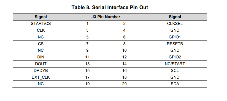
  • Ok, so is JP2 in position 2, JP20 in position 2, JP4 disconnected, JP24 where, JP21, JP22 & JP23 where? A table would save time ..

  • Jumper Name Settings
    JP2 VDD supplied from the 3rd pin
    JP4 Not installed 
    JP5 1st pin used as PWDN
    JP18 2-3
    JP19 1-2
    JP20 1-2 (GND)
    JP21 1-2
    JP22 2-3
    JP23 1-2
    JP24 VDD supplied from the 2nd pin

    This is the pin configuration that I use. 

  • Well, .. it is not very clear how you are powering the board. Maybe you could measure AVDD and AVSS & AGND which I think you are assuming are 3V and 0V. 

    JP2 VDD supplied from the 3rd pin That is 2.5V (or 5V) which requires an external 5V (Vcc_5V). Did you mean to supply 3V to JP2 middle (2nd) pin to provide 3V on AVDD?

    JP20 1-2 (GND) Does that mean an external wire to pin 2? AVSS must also be connected to AGND (or 2.5V which doesn't exist if there is no 5V) which looks like pin 2 to pin 3 not 1-2 (the schematic doesn't exactly make pin numbers clear)

      supply 3V to JP2 middle (2nd) pin to provide 3V on AVDD

    J3 connections? Why are these not all detailed

    JP21 1-2 means SPI_CS is on J3 pin 1
    JP22 2-3 means SPI_START is on J3 pin 14

  • Hi   thanks for your answer.  Yes, when I measure the voltage between AVSS, AVDD I see 3V.

    I didn't have a 5V external power supply and yes, I connect my 3V power supply to the VCC_5V side, not to the 2nd leg.

    JP20 1-2 means they are shorted. In the image I shared before, when I connected pins 1-2 together, AVSS was connected to GND. I did not share J3 part because there is no challenging part in there, I connected them directly to the microcontroller side defined pins.

Reply
  • Hi   thanks for your answer.  Yes, when I measure the voltage between AVSS, AVDD I see 3V.

    I didn't have a 5V external power supply and yes, I connect my 3V power supply to the VCC_5V side, not to the 2nd leg.

    JP20 1-2 means they are shorted. In the image I shared before, when I connected pins 1-2 together, AVSS was connected to GND. I did not share J3 part because there is no challenging part in there, I connected them directly to the microcontroller side defined pins.

Children
  • The symmetric voltage supply on the EK board can accept anything from ~3V to 5V DC and provide stable symmetric 2.5V to the chip (as long as the source can supply roughly 50mA). Adjust your jumpers to use the outputs from the LDOs, your description does not sound correct to me.

    It may be a good idea to draw your own schematic that includes the connections to the STM/NRF board(s).

    The ADS1299 absolutely refuses to work when the analog voltages or the pin config is not 100% correct.

  • Thank you for your help  and  . I haven't made any progress in this section so far. I think this is because I have problems feeding the ADS1299, and therefore, I can't communicate. While working on the coding, I also designed a PCB with the ADS1299 chip and the nRF52840 module as suggested by TI, and it arrived.

    I made the connections on the ADS1299 chip as follows:

    ADS1299 ------------------------- nRF52
    AVDD                                     VDD
    DVDD                                     VDD
    AVSS                                      GND
    CLKSEL                                  VDD
    DAISYIN                                 GND
    DRDY                                     P0.12
    SCK                                        P0.13
    MISO                                      P0.14
    MOSI                                      P0.15
    CS                                          P0.16
    START                                    P0.17
    RESET                                   P0.19
    PWDN                                    P0.20

    I measured the VCAP1 voltage, and it is above 1.1V, but I still cannot establish communication. ADS1299 returns 0x00 as a result. This is the latest library code that I created.

    #include "ADS1299_nRF.h"
    #include <nrf.h>
    #include <nrf_log.h>
    #include <nrf_log_ctrl.h>
    #include <nrf_log_default_backends.h>
    #include <nrf_gpio.h>
    #include <nrf_delay.h>
    #include "ads1299_delay.h"
    #include "nrfx_spim.h"
    
    // Enable polling mode for DRDY
    #define POLL_DREADY
    
    #define SPIM2 NRF_SPIM2
    #define ADS_POWER_RAMP_TIME_MSECS 30 // Delay for regulator to stabilize
    
    bool new_data_available = false;
    uint8_t rx_buffer[27], tx_buffer[8];
    uint8_t sample_number = 0;
    static uint8_t regData[24]; // Mirror of ADS1299 registers
    
    /** @brief SPI interface initialization. Accurate timing use HFCLK clock */
    void spi_init(void) {
        // Start HFCLK source for accurate timing
        NRF_CLOCK->TASKS_HFCLKSTART = 1;
        while (NRF_CLOCK->EVENTS_HFCLKSTARTED == 0);
        NRF_CLOCK->EVENTS_HFCLKSTARTED = 0;
        
        // Disable SPIM to configure it
        SPIM2->ENABLE = (SPIM_ENABLE_ENABLE_Disabled << SPIM_ENABLE_ENABLE_Pos);
        
        // Configure SPIM2 pins
        SPIM2->PSEL.SCK = ((PIN_SCK << SPIM_PSEL_SCK_PIN_Pos) |
                            (0 << SPIM_PSEL_SCK_PORT_Pos) |
                            (SPIM_PSEL_SCK_CONNECT_Connected << SPIM_PSEL_SCK_CONNECT_Pos));
    
        SPIM2->PSEL.MOSI = ((PIN_MOSI << SPIM_PSEL_MOSI_PIN_Pos) |
                            (0 << SPIM_PSEL_MOSI_PORT_Pos) |
                            (SPIM_PSEL_MOSI_CONNECT_Connected << SPIM_PSEL_MOSI_CONNECT_Pos));
    
        SPIM2->PSEL.MISO = ((PIN_MISO << SPIM_PSEL_MISO_PIN_Pos) |
                            (0 << SPIM_PSEL_MISO_PORT_Pos) |
                            (SPIM_PSEL_MISO_CONNECT_Connected << SPIM_PSEL_MISO_CONNECT_Pos));
        
        SPIM2->FREQUENCY = SPIM_FREQUENCY_FREQUENCY_M4; // 2 MHz (t_CLK = 500 ns)
        
        SPIM2->ORC = 0xFF;
    
        // ADS1299 set Data mode: clock polarity = 0, clock phase = 1
        SPIM2->CONFIG = (SPIM_CONFIG_CPOL_ActiveHigh << SPIM_CONFIG_CPOL_Pos) |  // CPOL = 0
                        (SPIM_CONFIG_CPHA_Trailing << SPIM_CONFIG_CPHA_Pos) |     // CPHA = 1
                        (SPIM_CONFIG_ORDER_MsbFirst << SPIM_CONFIG_ORDER_Pos);
        
        SPIM2->EVENTS_END = 0;
        SPIM2->EVENTS_ENDTX = 0;
        SPIM2->EVENTS_ENDRX = 0;
        
        SPIM2->INTENCLR = 0xFFFFFFFFUL;
        SPIM2->INTENSET = 0x040;
        
        SPIM2->ENABLE = (SPIM_ENABLE_ENABLE_Enabled << SPIM_ENABLE_ENABLE_Pos);
    }
    
    void gpio_init(void)
    {
        
        //NRF_P0->PIN_CNF[CS_PIN]   = 0x301;  // output, high drive high and low H0H1
        //NRF_P0->PIN_CNF[PIN_SCK]  = 0x301;  // output, high drive high and low H0H1
        //NRF_P0->PIN_CNF[PIN_MOSI] = 0x301;      // output, standard drive S0S1
        //nrf_gpio_cfg(PIN_MISO, NRF_GPIO_PIN_DIR_INPUT, NRF_GPIO_PIN_INPUT_DISCONNECT, NRF_GPIO_PIN_NOPULL, NRF_GPIO_PIN_H0H1, NRF_GPIO_PIN_NOSENSE);
        nrf_gpio_cfg(PWDN_PIN, NRF_GPIO_PIN_DIR_OUTPUT, NRF_GPIO_PIN_INPUT_DISCONNECT, NRF_GPIO_PIN_NOPULL, NRF_GPIO_PIN_H0H1, NRF_GPIO_PIN_NOSENSE);
        nrf_gpio_cfg(RESET_PIN, NRF_GPIO_PIN_DIR_OUTPUT, NRF_GPIO_PIN_INPUT_DISCONNECT, NRF_GPIO_PIN_NOPULL, NRF_GPIO_PIN_H0H1, NRF_GPIO_PIN_NOSENSE);
        nrf_gpio_cfg_input(PIN_DRDY, GPIO_PIN_CNF_PULL_Pullup);	
        nrf_gpio_pin_clear(CS_PIN);
        nrf_delay_ms(50);
        nrf_gpio_pin_set(CS_PIN);
        nrf_delay_ms(10);
    
    
    }
    
    static void spi_uninit(void) {
        SPIM2->ENABLE = (SPIM_ENABLE_ENABLE_Disabled << SPIM_ENABLE_ENABLE_Pos);
        nrf_gpio_cfg_input(PIN_SCK, NRF_GPIO_PIN_NOPULL);
        nrf_gpio_cfg_input(PIN_MOSI, NRF_GPIO_PIN_NOPULL);
        nrf_gpio_cfg_input(PIN_MISO, NRF_GPIO_PIN_NOPULL);
    }
    
    bool spi_transfer_byte(uint8_t *tx, uint8_t *rx, size_t len) {
        if (!(SPIM2->ENABLE & SPIM_ENABLE_ENABLE_Msk)) {
            SPIM2->ENABLE = (SPIM_ENABLE_ENABLE_Enabled << SPIM_ENABLE_ENABLE_Pos);
        }
    
        SPIM2->EVENTS_END = 0;
        SPIM2->TXD.PTR = (uint32_t)tx;
        SPIM2->TXD.MAXCNT = len;
        SPIM2->RXD.PTR = (uint32_t)rx;
        SPIM2->RXD.MAXCNT = len;
    
        SPIM2->TASKS_START = 1;
        while (!SPIM2->EVENTS_END);
    
        SPIM2->TASKS_STOP = 1;
        while (!SPIM2->EVENTS_STOPPED);
    
        NRF_LOG_INFO("SPI TX: 0x%02x, RX: 0x%02x", tx[0], rx ? rx[0] : 0);
        return true;
    }
    
    bool spi_transfer_bytes(const uint8_t *tx, uint8_t *rx, size_t len) {
        if (!(SPIM2->ENABLE & SPIM_ENABLE_ENABLE_Msk)) {
            SPIM2->ENABLE = (SPIM_ENABLE_ENABLE_Enabled << SPIM_ENABLE_ENABLE_Pos);
        }
        
        static uint8_t dummy_tx = 0xFF;
        static uint8_t dummy_rx;
    
        SPIM2->EVENTS_END = 0;
        SPIM2->TXD.PTR = (uint32_t)(tx ? tx : &dummy_tx);
        SPIM2->TXD.MAXCNT = len;
        SPIM2->RXD.PTR = (uint32_t)(rx ? rx : &dummy_rx);
        SPIM2->RXD.MAXCNT = len;
    
        SPIM2->TASKS_START = 1;
        while (!SPIM2->EVENTS_END);
        SPIM2->ENABLE = SPIM_ENABLE_ENABLE_Disabled; // Disable SPIM to allow pull-up to take effect
        return true;
    }
    
    void ADS1299_pwr_up_seq(void) {
    
        nrf_gpio_pin_set(PWDN_PIN); // Power on
        nrf_gpio_pin_set(RESET_PIN); // Reset low
        nrf_delay_ms(150);          // Wait for tPOR
    
        nrf_gpio_pin_clear(RESET_PIN); // Reset low
        nrf_delay_us(2);             // ≥2 clock cycles
        nrf_gpio_pin_set(RESET_PIN);  // Reset high
        nrf_delay_ms(10);              // Stabilization
    }
    
    void Reset_ADS(void)
    {
    	nrf_gpio_pin_set(PWDN_PIN);
    	nrf_delay_us(100000);
    	nrf_gpio_pin_clear(PWDN_PIN);
    	nrf_delay_us(100000);
    	nrf_gpio_pin_set(PWDN_PIN);
    	nrf_delay_us(100000);
    }
    
    bool ADS1299_init(void) {
        // Recommended power-up sequence for ADS1299
        
        NRF_LOG_INFO("Initializing ADS1299");
        //Reset_ADS();
        ADS1299_pwr_up_seq();
            
        NRF_LOG_INFO("SPI init success");
    #ifdef POLL_DREADY
        NRF_LOG_INFO("DRDY polling enabled");
    #else
        NRF_LOG_INFO("DRDY interrupt not implemented");
    #endif
        return true;
    }
    
    void poll_dready(void) {
    #ifdef POLL_DREADY
        NRF_LOG_INFO("Polling DRDY, state: %d", nrf_gpio_pin_read(PIN_DRDY));
        if (nrf_gpio_pin_read(PIN_DRDY) == 0) {
            NRF_LOG_INFO("DRDY low, receiving data");
            ADS1299_receive_data();
            send_new_available_data();
        }
    #endif
    }
    
    bool ADS1299_write_register(uint8_t address, uint8_t value) {
    
        uint8_t cmd[] = {
            (uint8_t)(address | COMMAND_WREG),
            0x00, // Write 1 register
            value
        };
    
        nrf_gpio_pin_clear(CS_PIN);
        nrf_delay_us(2); // t_CSSC: Delay from CS low to first SCLK (min 6 ns, use 50 ns for safety)
        spi_transfer_byte(cmd, NULL, 3);
        nrf_delay_us(2); // t_CSH: Delay from last SCLK to CS high (min 1 µs)
        nrf_gpio_pin_set(CS_PIN);
        nrf_delay_us(1); // t_CSH hold time after CS high
    
        regData[address] = value;
        return true;
    }
    
    uint8_t ADS1299_read_reg(uint8_t address) {
        uint8_t tx_data = 0x20 | address;  // RREG command (0x20) + address
        uint8_t dummy = 0x00;
        uint8_t rx_data = 0;
        
        // Pull CS low to start transaction
        nrf_gpio_pin_clear(CS_PIN);
        
        // Send RREG command + address (transmit only)
        spi_transfer_byte(&tx_data, NULL, 1);
        nrf_delay_us(2);
        
        // Send dummy byte and receive register data
        spi_transfer_byte(&dummy, &rx_data, 1);
        nrf_delay_us(2);
        
        // Pull CS high to end transaction
        nrf_gpio_pin_set(CS_PIN);
        
        // Store in global array if you're using it
        regData[address] = rx_data;
        
        return rx_data;  // Return the register value directly
    }
    
    bool ADS1299_send_command(uint8_t command) {
        uint8_t dummy;
        nrf_gpio_pin_clear(CS_PIN);
        spi_transfer_byte(&command, NULL, 1);
        nrf_delay_us(2);
        nrf_gpio_pin_set(CS_PIN);
        nrf_delay_us(2); // t_CSH hold time after CS high
        return true;
    }
    
    bool ADS1299_send_start(void) {
        bool result = ADS1299_send_command(COMMAND_START);    
        return result;
    }
    
    bool ADS1299_send_read_continuous(void) {
        bool result = ADS1299_send_command(COMMAND_RDATAC);
        nrf_delay_us(3); // Allow RDATAC to settle
        return result;
    }
    
    bool ADS1299_send_reset(void) {
        bool result = ADS1299_send_command(COMMAND_RESET);
        NRF_LOG_INFO("Reset command sent, result: %d", result);
        return result;
    }
    
    bool ADS1299_send_sdatac(void) {
        bool result = ADS1299_send_command(COMMAND_SDATAC);
        NRF_LOG_INFO("Stop read continuously command sent, result: %d", result);
        return result;
    }
    
    bool ADS1299_receive_data(void) {
        new_data_available = false;
        if (!spi_transfer_bytes(NULL, rx_buffer, 27)) {
            NRF_LOG_ERROR("Failed to receive data");
            return false;
        }
        new_data_available = true;
        NRF_LOG_INFO("Data received, triggering send_new_available_data");
        return true;
    }
    
    bool ADS1299_poll_new_data(ADS1299_data_t *data) {
        if (new_data_available) {
            new_data_available = false;
            *data = ADS1299_convert_data();
            return true;
        }
        return false;
    }
    
    static inline int32_t buffer_to_channel(uint8_t id) {
        int32_t value = (rx_buffer[3 + id * 3] << 16) | (rx_buffer[4 + id * 3] << 8) | rx_buffer[5 + id * 3];
        if (value & 0x00800000) {
            value |= 0xFF000000;
        } else {
            value &= 0x00FFFFFF;
        }
        return value;
    }
    
    ADS1299_data_t ADS1299_convert_data(void) {
        ADS1299_data_t data;
        data.lead_off_positive = rx_buffer[0] << 4;
        data.lead_off_positive |= (rx_buffer[1] & 0b11110000) >> 4;
        data.lead_off_negative = rx_buffer[1] << 4;
        data.lead_off_negative |= (rx_buffer[2] & 0b11110000) >> 4;
        data.gpio_0 = rx_buffer[2] & 0b00001000;
        data.gpio_1 = rx_buffer[2] & 0b00000100;
        data.gpio_2 = rx_buffer[2] & 0b00000010;
        data.gpio_3 = rx_buffer[2] & 0b00000001;
        data.channel_0 = buffer_to_channel(0);
        data.channel_1 = buffer_to_channel(1);
        data.channel_2 = buffer_to_channel(2);
        data.channel_3 = buffer_to_channel(3);
        data.channel_4 = buffer_to_channel(4);
        data.channel_5 = buffer_to_channel(5);
        data.channel_6 = buffer_to_channel(6);
        data.channel_7 = buffer_to_channel(7);
        return data;
    }
    
    void send_new_available_data(void) {
        if (new_data_available) {
            new_data_available = false;
            NRF_LOG_INFO("Sample: %d", sample_number++);
            for (uint8_t i = 0; i < 27; i++) {
                NRF_LOG_INFO("Byte %d: 0x%02x", i, rx_buffer[i]);
            }
        }
    }


    This is the main part.
    #include <nrf.h>
    #include <nrf_log.h>
    #include <nrf_log_ctrl.h>
    #include <nrf_log_default_backends.h>
    #include "ADS1299_nRF.h"
    #include "nrf_delay.h"
    #include "nrf_gpio.h"
    
    
    extern bool new_data_available;
    
    int main(void) {
        NRF_LOG_INIT(NULL);
        NRF_LOG_DEFAULT_BACKENDS_INIT();
    
        NRF_LOG_INFO("Starting ADS1299 initialization");
        
        gpio_init();
        spi_init();
        if (!ADS1299_init()) 
        {
            NRF_LOG_ERROR("ADS1299 init failed");
            while (1) {
                //nrf_gpio_pin_toggle(LED_PIN);
                NRF_LOG_FLUSH();
                nrf_delay_ms(200);
            }
        }
        
        ADS1299_send_reset();
        nrf_delay_ms(1);
        ADS1299_send_sdatac();
        uint8_t id = 0x00;
    
        id = ADS1299_read_reg(ID);
    
        if (id == 0x3E) 
        {
            NRF_LOG_INFO("ADS1299 communication success, ID: 0x%02x", id);
        }
        else 
        {
            NRF_LOG_INFO("ADS1299 communication fail, ID: 0x%02x", id);
        }
    }


    Thank you for your suggestions and help so far. It would be easier to reach the problem through a card that has been put together rather than trying to debug the problem through DK.

  • Re-read the ADS1299 datasheet. It clearly stated in chapter 7.3 that you need at least 4.75V between AVDD and AVSS.

    Unsurprisingly the chip won't work when your supply is significantly below that.

    Sounds like you need to redesign your board...

  • Thanks for your reply. I did not pay attention to that part. I can add a voltage regulator to that part.  With this problem, I go back to the starting point. Is there any misconfiguration present in my code? Any misleading operation? Thanks again  .

  • Now, I go back to the ADS board, I am not using the MMB0 board. I supplied DVDD with the nRF VDD, and for the AVDD, I am giving 5V externally. 


    These are the pin connections that I did in my configuration. I have mentioned the code I tried above. What am I doing wrong? Thanks for your replies   and  .


Related