
Hello,
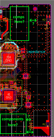
I am working on a prototype board based on the nRF7002 DK. I have managed to preserve the entire PCB layout sections for the nRF5340 and nRF7002 radios and antenna without modification. However, I have a lot of application hardware to add around this in a small form factor. Can anyone advise as to whether or not I can add other application circuitry in the green boxes as shown below? I'm basically trying to understand what a reasonable rule of thumb is for the green "?" clearance distances between arbitrary application circuitry and the antenna planar void section (top of graphic) and the guarded RF signal feed (lower part of graphic).
Thank you in advance,
Chris

