Request to review schematic and hardware layout

Hi there, I've been told on Reddit that I can post my design here to receive more relevant feedback.

I'm making a module with nRF54L15 with an external DC-DC regulator to keep the efficiency at maximum.

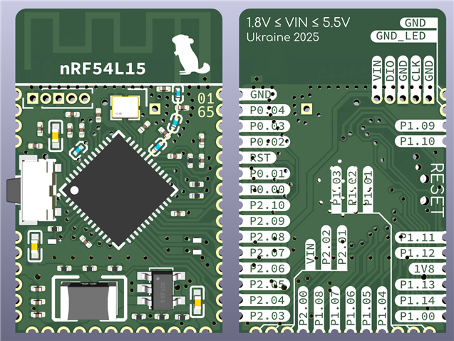
The MCU schematic is mostly a copy-paste of the reference design, the layout isn't though.

I would appreciate any comments and criticism!

Github (KiCad): https://github.com/efogdev/nrf54l15-module

KiCanvas: https://kicanvas.org/?github=https%3A%2F%2Fgithub.com%2Fefogdev%2Fnrf54l15-module

Just pictures: https://postimg.cc/gallery/8j2K1C9 (edit: please use github and kicanvas as some changes have already been made).

P.S. One more question, am I doing something wrong? I have never seen an antenna trace so thin, usually it's 0.3mm and more. 0.12mm looks weird to me. Also if I use another calculator, I get value of 0.19mm.

Parents
  • Hello Artem,

    Schematic:
    C13, C14 and C15 on RESET line?


    Layout:
    Match layout -> update it to copy the one from our reference layout here: nsscprodmedia.blob.core.windows.net/.../pca10156-nrf54l15-dk-0_9_1.zip pay attention to the structures and notes related to the RF matching components. There's a single GND island for your C8 that is recommended. Make the RF match in a straight line and then have a 50Ohm wave guide if needed to the antenna input.
    Remove copper under match on In1 and In2. This is important to ensure equal and reduced stray capacitance between the matching network and the inner layer GND copper. You have a line running from U6 under the matching network. I'd recommend using In1 to route this up to the connection towards the antenna part of the board. Run the trace perpendicular to the traces running across the board on In2 and avoid running the power under the matching network. This way you can remove the inner layer cutout under the matching network as well.


    Otherwise I think it looks ok.


    Best regards
    Asbjørn

  • Thanks, Asbjørn!

    C13, C14 and C15 on RESET line?

    Just didn't want to introduce a new BOM position for the RC network (from the reference design in the datasheet). It is really necessary though? Also, is the ferrite bead still necessary when the internal switching regulator is off?

    Everything else makes sense!

    edit: also, do I understand correctly that the matching network must be as physically small as possible and be placed as close to the antenna pin as possible? While I would prefer a working product, I don't want to copy the layout blindly.

Reply
  • Thanks, Asbjørn!

    C13, C14 and C15 on RESET line?

    Just didn't want to introduce a new BOM position for the RC network (from the reference design in the datasheet). It is really necessary though? Also, is the ferrite bead still necessary when the internal switching regulator is off?

    Everything else makes sense!

    edit: also, do I understand correctly that the matching network must be as physically small as possible and be placed as close to the antenna pin as possible? While I would prefer a working product, I don't want to copy the layout blindly.

Children
  • Hi Artem,

    If you are not using the DCDC at all, then the components related to it can be skipped, but that will drop the efficiency quite a bit. So we recommend customers to include the ferrite, inductors and caps related to the DCDC for performance.

    The RESET cap only need to be one, so I was confused as to why you had three component footprints.

    The matching network should be placed as close to the chip as possible and we do recommend copying the layout. It's important to reproduce the peformance. 1mm of trace length or via at 2.4Ghz is about 1nH of inductance and this along with the stray capacitance between these components and GND are factored into the component and placement selection and reference design we have. 

    Best regards

    Asbjørn

Related