Antenna connection

Hi, 

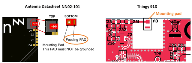
why antenna trace is connected to mounting pad instead of feeding pad of antenna in thingy 91x

We are designing our device based on this. We wish to be sure about this.

regards

Vivek

  • NRF9151-5-6.pdf

    2. Please see our schematics for the antenna and verify.

    regards

    Vivek

  • Hi Vivek, 

    Regarding the chip antenna placement, if you check the manufacturer data sheet for "NN02-101" there are two suggested ways of placing the chip antenna, one for placing chip antenna in the middle of PCB and another is to place chip antenna on the edge (corner) of PCB. For Thingy 91X the chip antenna is placed on the edge of PCB so the feeding pad is selected accordingly from antenna chip manufacturer suggestion. 

  • Hi Vivek,

    Regarding the schematic review, I see that you are using nRF54L15 for 2.4 GHz part, because I don't have the layout, I cannot have a full overview over the RF matching and antenna placement part. It would be great if you could share layout as well. Other than that, just be aware that the antenna matching network in your schematic (C44, C48,L7, L8) are selected based on Thingy91X PCB structure, so if you have different PCB size, or placement of other components might affect the antenna performance and you might need to tune it for your own PCB. Here is a documentation from antenna manufacturer about antenna matching selection based on PCB. I would recommend to follow the guidance from that for optimal antenna matching. 
    AN_Different-ground-plane-form-factors-with-Ignions-NANO-PCBs.pdf

    Also make sure to place the Chip matching network as similar as reference design layout for nRF54L15. Please share your crystal part number or datasheet if you want to check spec for that as well.  

Related