The BLE stack causes the SPI pin waveforms to be different.

I'm develping my application with nrf52832 and nrf SDK v17.

I'm testing SPI interface so that I can use the external flash.

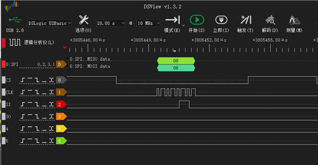
When I using SPI without BLE stack,the waveform looks like this:

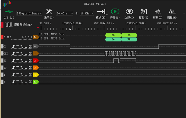
But when I add BLE stack to application,the wave form changed..It looks like this:

The relevant code being executed when the situation shown in the figure occurred is as follows

void hal_spi_init(void)
{
	nrf_drv_spi_config_t spi_config = NRF_DRV_SPI_DEFAULT_CONFIG;
    spi_config.ss_pin   = SPI_SS_PIN;
    spi_config.miso_pin = SPI_MISO_PIN;
    spi_config.mosi_pin = SPI_MOSI_PIN;
    spi_config.sck_pin  = SPI_SCK_PIN;
    APP_ERROR_CHECK(nrf_drv_spi_init(&spi, &spi_config, spi_event_handler, NULL));
}

void SpiFlash_WriteOneByte(uint8_t Dat)
{
    uint8_t len = 1;
    spi_tx_buf[0] = Dat;
	spi_xfer_done = false;
	APP_ERROR_CHECK(nrf_drv_spi_transfer(&spi, spi_tx_buf, len, spi_rx_buf, len));
    while(!spi_xfer_done)
			;
}

void SpiFlash_Write_Enable(void)
{
    spi_xfer_done = false;
	  SpiFlash_WriteOneByte(SPIFlash_WriteEnable_CMD);
	  while(!spi_xfer_done)
			;
}

void SPIFlash_Erase_Sector(uint8_t Block_Num,uint8_t Sector_Number)
{
    SpiFlash_Write_Enable();
		
	  spi_tx_buf[0] = SPIFlash_SecErase_CMD;
	  spi_tx_buf[1] = Block_Num;
	  spi_tx_buf[2] = Sector_Number<<4;
	  spi_tx_buf[3] = 0x00;
	  spi_xfer_done = false;
		APP_ERROR_CHECK(nrf_drv_spi_transfer(&spi, spi_tx_buf, 4, spi_rx_buf, 4));
		while(!spi_xfer_done)
			;	
    nrf_delay_ms(10);

    return ;
}

uint8_t SpiFlash_Write_Page(uint8_t *pBuffer, uint32_t WriteAddr, uint32_t WriteBytesNum)
{
    uint8_t len;
	
	  SpiFlash_Write_Enable();
		
    spi_tx_buf[0] = SPIFlash_PageProgram_CMD;
	  spi_tx_buf[1] = (uint8_t)((WriteAddr&0x00ff0000)>>16);
	  spi_tx_buf[2] = (uint8_t)((WriteAddr&0x0000ff00)>>8);
	  spi_tx_buf[3] = (uint8_t)WriteAddr;
	
	  memcpy(&spi_tx_buf[4],pBuffer,WriteBytesNum);
	
	  len = WriteBytesNum + 4;
	  spi_xfer_done = false;
		APP_ERROR_CHECK(nrf_drv_spi_transfer(&spi, spi_tx_buf, len, spi_rx_buf, 0));
    while(!spi_xfer_done)
			;	

    return RET_SUCCESS;
}

uint8_t SpiFlash_Read(uint8_t *pBuffer,uint32_t ReadAddr,uint32_t ReadBytesNum)
{
    uint8_t len;
		
		spi_tx_buf[0] = SPIFlash_ReadData_CMD;
	  spi_tx_buf[1] = (uint8_t)((ReadAddr&0x00ff0000)>>16);
	  spi_tx_buf[2] = (uint8_t)((ReadAddr&0x0000ff00)>>8);
	  spi_tx_buf[3] = (uint8_t)ReadAddr;
		
		len = ReadBytesNum + 4;
	  spi_xfer_done = false;
		APP_ERROR_CHECK(nrf_drv_spi_transfer(&spi, spi_tx_buf, len, spi_rx_buf, len));
	  while(!spi_xfer_done)
			;	
    memcpy(pBuffer,&spi_rx_buf[4],ReadBytesNum);
    
    return RET_SUCCESS;
}

    hal_spi_init();
    nrf_delay_ms(100);
    SPIFlash_Erase_Sector(0,0);
    nrf_delay_ms(100);
    flash_tx_buf[0] = 0;flash_tx_buf[1] = 0;flash_tx_buf[2] = 0;flash_tx_buf[3] = 0;flash_tx_buf[4] = 1;
    SpiFlash_Write_Page(flash_tx_buf,0x00,5);
    
    SpiFlash_Read(flash_rx_buf,0x00,5);

Parents
  • First note that the DSView is showing poor signals, in particular the clock is not consistent, which may be due to low DSView sampling rate but is often also due to slow rising and falling edges as you are using default low-drive on the 3 SPI outputs. Fix by adding H0H1 settings after the SPI init:

    void hal_spi_init(void)
    {
    	nrf_drv_spi_config_t spi_config = NRF_DRV_SPI_DEFAULT_CONFIG;
        spi_config.ss_pin   = SPI_SS_PIN;
        spi_config.miso_pin = SPI_MISO_PIN;
        spi_config.mosi_pin = SPI_MOSI_PIN;
        spi_config.sck_pin  = SPI_SCK_PIN;
        APP_ERROR_CHECK(nrf_drv_spi_init(&spi, &spi_config, spi_event_handler, NULL));
        // Configure SPI output pins to be High Drive (H0H1) to get improved edges
        nrf_gpio_cfg(SPI_SS_PIN,   NRF_GPIO_PIN_DIR_OUTPUT, NRF_GPIO_PIN_INPUT_CONNECT, NRF_GPIO_PIN_NOPULL, NRF_GPIO_PIN_H0H1, NRF_GPIO_PIN_NOSENSE);
        nrf_gpio_cfg(SPI_MOSI_PIN, NRF_GPIO_PIN_DIR_OUTPUT, NRF_GPIO_PIN_INPUT_CONNECT, NRF_GPIO_PIN_NOPULL, NRF_GPIO_PIN_H0H1, NRF_GPIO_PIN_NOSENSE);
        nrf_gpio_cfg(SPI_SCK_PIN,  NRF_GPIO_PIN_DIR_OUTPUT, NRF_GPIO_PIN_INPUT_CONNECT, NRF_GPIO_PIN_NOPULL, NRF_GPIO_PIN_H0H1, NRF_GPIO_PIN_NOSENSE);
        // Configue SPI inout pin to have pull-up enabled in case slave device is not connected
        nrf_gpio_cfg(SPI_MISO_PIN, NRF_GPIO_PIN_DIR_INPUT,  NRF_GPIO_PIN_INPUT_CONNECT, NRF_GPIO_PIN_PULLUP, NRF_GPIO_PIN_S0S1, NRF_GPIO_PIN_NOSENSE);
    }
    

    Next note that there is an Errata 58 when applies trying to use a single byte transfer, which is affected by many things including day of the week:

    3.9 [58] SPIM: An additional byte is clocked out when RXD.MAXCNT = 1
     Symptoms
       SPIM clocks out additional byte.
     Conditions
       RXD.MAXCNT = 1
       TXD.MAXCNT <= 1
     Consequences
       Additional byte is redundant

    Fix: don't use single byte transfers or just ignore extra byte (without crashing stack ..)

  • The slave of spi is external SPI flash.It seem a It seems to strictly require a one-byte Write Enable command.

    Is there any other way to solve the second point you mentioned above?

Reply Children
  • Given that there is no actual data being read back when using a Write Enable command, perhaps try setting RXD.MAXCOUNT to 0.

    void SpiFlash_WriteOneByte(uint8_t Dat)
    {
        uint8_t len = 1;
        spi_tx_buf[0] = Dat;
    	spi_xfer_done = false;
    	// Only for Write Enable command, set Rx len to 0
    	APP_ERROR_CHECK(nrf_drv_spi_transfer(&spi, spi_tx_buf, len, spi_rx_buf, 0));
        while(!spi_xfer_done)
    			;
    }
    

Related