Hi all, hope this is the right place.
I'm developing a small breakout board to test/program the NRF52805; this board will eventually be expanded to include a pressure sensor and a PMIC (ideally Nordic too). I'm fairly new to more complex board design, and would appreciate any/all feedback. Please keep in mind I'm also working around a lot of the constraints set by JLCPCB/easyEDA in my design.
Points I've tried to keep in mind:
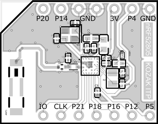
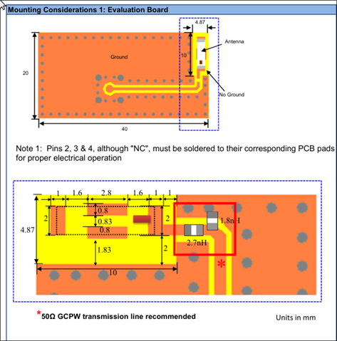
- Nordic reference circuit is followed as closely as possible (which has been an excellent resource - some minor adjustments to accommodate for breakout pad routing).
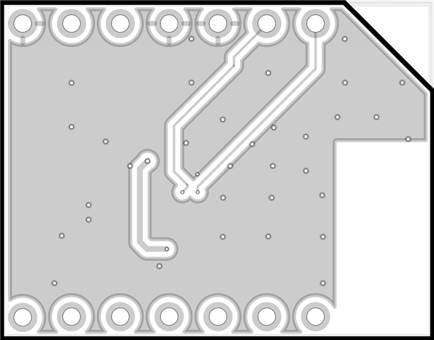
- Board is two-layer, FR4, ground pours on each.
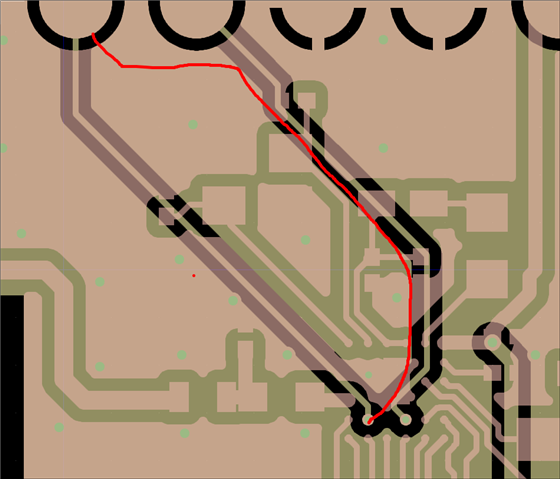
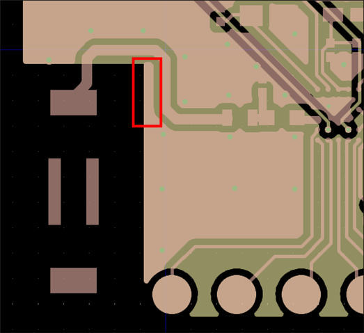
- Stitching/suture vias are as close to reference design as possible - vias on grounds, and closer vias around antenna feed. Otherwise vias are spaced out ~3mm.
- Antenna is a chip antenna, where clearance follows manufacturer specs; I'm aware I'm sacrificing quite a bit, given the reduced size of the board and GND, but in the future I plan on implementing a larger meandering-type design on a separate flexible PCB, more aligned to the project's needs. The biggest question is whether or not I need a separate matching/tuning circuit for the antenna: it is 50ohm already, and the manufacturer doesn't seem to suggest the need for anything beyond the trace (Johanson's eval board circuits seem to include only tuning for the specific eval board, and not general prescriptions, or at least that's the case with the majority of their components - https://lcsc.com/datasheet/lcsc_datasheet_2411220415_Johanson-Dielectrics-2450AT43B100E_C2917721.pdf).
Points I've got questions about:
- General viability as initial prototype (i.e. will the damn thing work at all). I expect to be refining the design over many iterations,
- The central GNDs (6) on the NRF52805; should these all be via-in-pads? At the moment I've got them all connected via a section of GND pour and a via to the bottom GND.
Thank you very much in advance -
Niko