Hi
I have some questions about nRF5340 & nPM1300 decoupling cap
nRF5340
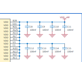
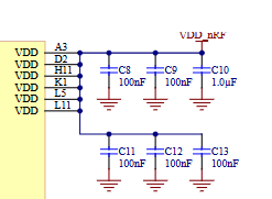
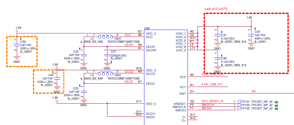
1.For pin A3/D2/H11/K1/L5/L11, ref. SCH is 1uF*1 and 0.1uF*5, could we only connect 1uF*1 and 0.1uF*2?
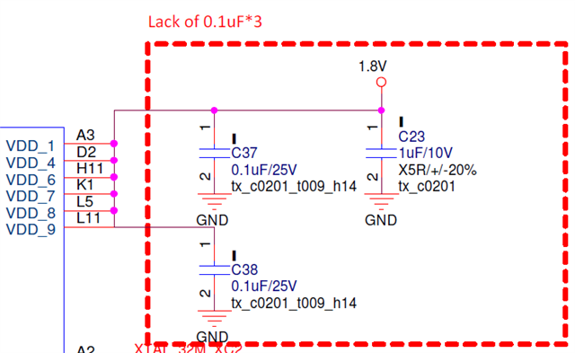
2.For consider all VDD pin(A3/D2/H11/K1/L5/L11/B7/B10/E11/B12), could we connect 1uF*3 and 0.1uF*2?
nPM1300
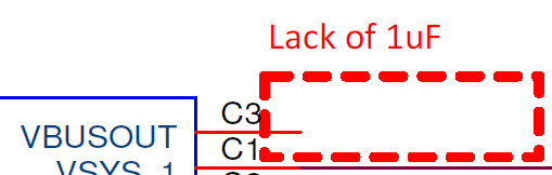
1.We don't use pin C3 VBUSOUT function, could we let C3 pin floating?
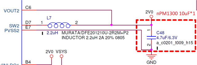
2.Pin C6 VOUT2 ref. SCH is 10uF*1,could we connect 4.7uF*1?
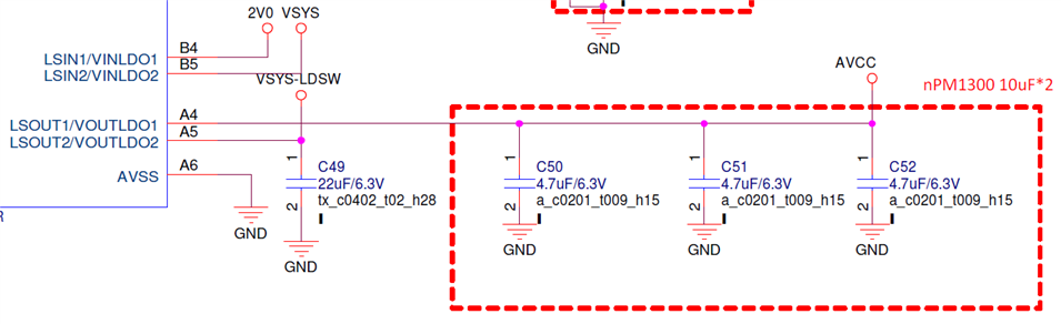
3.Pin A4 LSOUT1/VOUTLDO1 ref. SCH is 10uF*2,could we connect 4.7uF*3?
Thank you
Poki