Fabrication Drawing Questions for nRF7002DK

Hello,

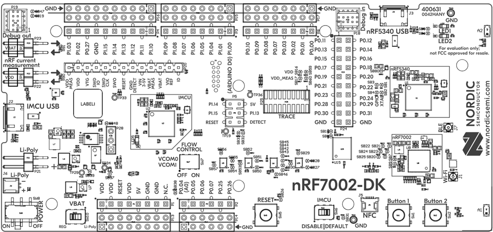
I am designing a custom PCBA based on the nRF7002DK PCBA and I really need the Fabrication Notes / Drawing that officially went to the fabricator to direct the build, if possible, please. I am getting push-back from my NPI prototype vendor regarding capabilities limitations for the nRF5340 via-in-pad construction.

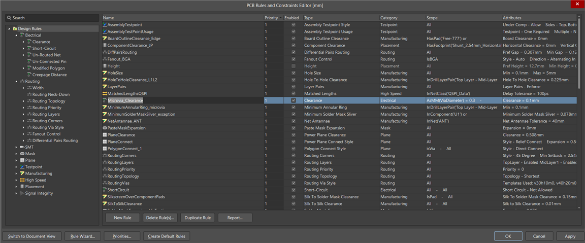
At this point I've made only one change to the L1-L2 microvia spec to ease minimum soldermask sliver between BGA pads. I changed the via diameter from 0.3mm to 0.254mm. This continues to meet standard class 2 minimum annular ring for a 4 mil laser drill, so I think it's ok. Let me know if you disagree.

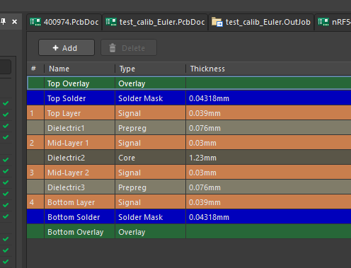
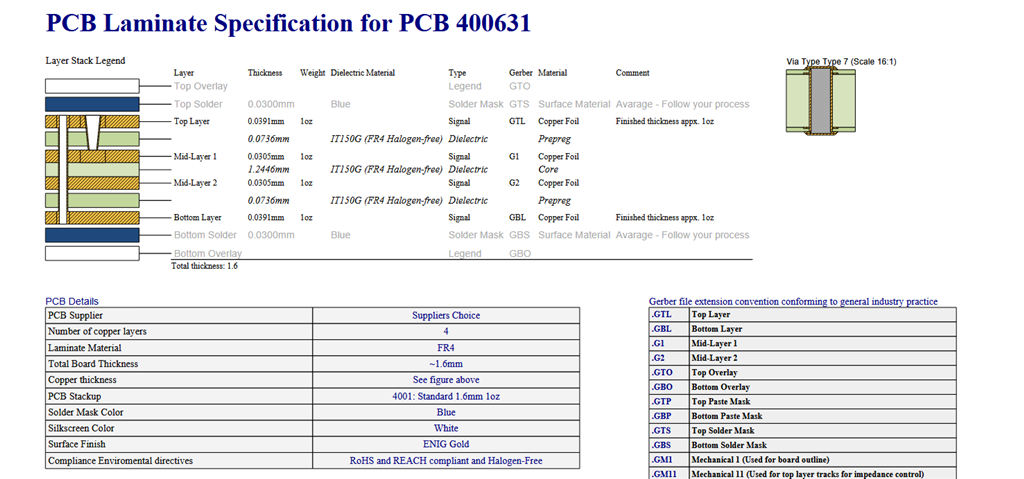
Also regarding the stack-up in the DK Altium files, and with respect to the microvias, there is an aspect ratio problem. For the stack-up in the Altium files, the effective aspect ratio is about 1.45:1. Max permitted aspect ratio for a 4 mil laser drilled microvia is 1:1. So, I don't know how Nordic managed to manufacture the DK with this stackup. Maybe the Altium stackup is not what's in the fab drawing. You can see what I'm getting at here now.

In addition to all of this, I want to be very clear about specifying the board is generally class 2 but requires special considerations for the nRF5340 only. Here's what I have in my draft fabrication notes as of right now specifically related to this:

General Construction Notes

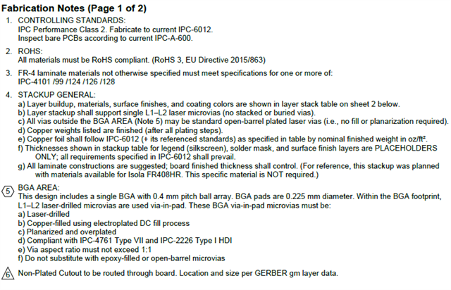
  • Build to IPC-6012 Class 2 performance requirements unless otherwise specified.

  • Layer stackup shall support single L1–L2 laser microvias (no stacked or buried vias).

  • All vias outside of the BGA area may be standard open-barrel plated laser vias (i.e., no fill or planarization required).


BGA Area (HDI Exception Handling)

  • This design includes a single BGA with 0.4 mm pitch ball array. BGA pads are 8.858 mil diameter (circular).

  • Within the BGA footprint, L1–L2 laser-drilled microvias are used via-in-pad.

  • These BGA via-in-pad microvias must be:

    • Laser-drilled

    • Copper-filled using electroplated DC fill process

    • Planarized and overplated

    • Compliant with IPC-4761 Type VII and IPC-2226 Type I HDI

    • Via aspect ratio must not exceed 1:1

    • Do not substitute with epoxy-filled or open-barrel microvias


Stackup Adjustment Request


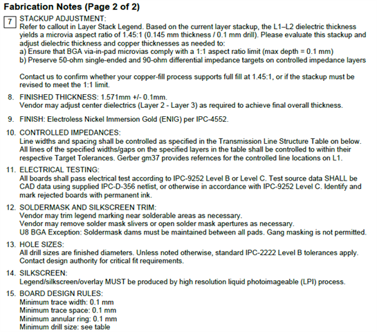
  • Based on the current layer stackup, the L1–L2 dielectric thickness yields a microvia aspect ratio of 1.45:1 (via drill = 3.937 mil, pad = 10 mil).

  • Please evaluate this stackup and adjust dielectric thickness and copper thicknesses as needed to:

    • Ensure that BGA via-in-pad microvias comply with a 1:1 aspect ratio limit (max depth = 3.937 mil)

    • Preserve 50-ohm single-ended and 90-ohm differential impedance targets on controlled impedance layers

  • Contact us to confirm whether your copper-fill process supports full fill at 1.45:1, or if the stackup must be revised to meet the 1:1 limit.


I ask that someone from Nordic engineering please review this and provide me with any additional instructions I need to ensure I accurately communicate Nordic's full fabrication intent to my NPI vendor.

Thank you in advance,

Chris

Parents
  • Hello Chris,
    Sorry for the delay here, we're a bit short now during summer holidays in Norway and your question is a bit unusual, so  I had to get some input from others. 
    Q1: First of all, which files and versions are you looking at, just so I'm sure. I've been looking at the nRF7002-DK hardware files version 0.7.2 now from here: https://www.nordicsemi.com/Products/Development-hardware/nRF7002-DK/Download
    The nRF7002 DK is the development kit for the nRF7002, and nRF7001 Wi-Fi 6 Companion ICs. It contains everything needed to get started developing on a single board. The DK features an nRF5340 multiprotocol System-on-Chip (SoC) as a host processor for the nRF7002. The DK supports the development of low-power Wi-Fi applications and enables Wi-Fi 6 features like OFDMA, Beamforming, and Target ...
    www.nordicsemi.com
    In them in Altium you'll find the stack up like this one:
    We have 0.1mm microvia holes.
    We have 0.76mm between top and mid layer 1 in the stack up. 0.100mm is not a concern, only check the impedance calculations where that is important.
    The adjusted microvia from 0.3mm to 0.254mm is ok
    Q2: The aspect ration, we're not really sure if we understand what you are referencing here. Are you able to share some screen shots indicating where and what you are looking at?
    In the HW files you'll find the files we send to our manufacturer.
    With all that said, I don't think I've really answered your questions properly, I fear there's a misunderstanding here with what is "wrong" with your production files. If you share the HW files for the development kit with your NPI vendor, are they seeing the same issues and concerns? Just as a reference point I mean.
    Best regards
    Asbjørn
  • Hi Asbjom,

    I'm sorry for my delayed response. I am at the point where my PCBA is in fabrication / assembly and all manufacturing issues have been addressed with my vendor. I just wanted to see if there were any specific fabrication instructions from Nordic's side. I'll answer your individual questions now.

    Q1. Correct, I am using the files from the 7002DK. The Fabrication folder only has Gerbers. PCB fabrication data usually includes a fabrication drawing that specifies things like controlling standards, finishes, drill tolerances, testing, and callouts for features and items that need special attention, among other things. I was specifically requesting this document, if you have one, so that I can see if any special instructions are warranted.

    Q2. Typically, laser microvias with aspect ratios larger than 1:1 are difficult to fill and plate. My vendor listed 1:1 as a limit on their capabilities sheet. The stack-up for the 7002DK creates a 1.45:1 L1-L2 laser microvia if you add up the thicknesses: 

    L1 + Dielectric + L2 = 0.039 + 0.076 + 0.03 = 0.145mm numerator
    The denominator is the hole size = 4 mil = 0.1016mm

    So, the aspect ratio for the microvia with this stackup is 0.145 / 0.1016 = 1.43:1 which exceeds 1:1.

    When I got down to asking my vendor about this in the end they said they could fill and plate this aspect ratio, so it is no longer an "issue" from my perspective.

    Those were really the only two concerns. If you do happen to have a PDF fabrication drawing that was sent to your PCB vendor in addition to the Gerbers and would be willing to share it with me I would very much appreciate it.

    Beyond that, we can close this issue now.

    Thank you,
    Chris

  • Hi Chris,
    Q1: 
    There's a rules section in Altium, but it's not this that you are looking for?
    We have the stack up details here, but I'm not sure if this is what you are looking for either?
    Just since you write fabrication drawing. This is what we refer to as assembly drawing>
    Is any of this the right information for you?
    Q2: Are you confident with that information? We do occasionally get some assembly/PCB manufacturer question and sometimes there seems to be a difference in terminology used for various aspects and it take two/three rounds before the right persons understand what's in play. 
    Best regards
    Asbjørn
  • I have a similar query about the reference layout for the NRF54L15 caaa chip. The layer stackup there has similar thicknesses -- .08mm for the L1-L2 dielectric and .035 mm for L1 thickness. The reference design has a microvia hole size of .1 mm and a pad diameter of only .2 mm. That gives us an annular ring of 50 um and a hole aspect ratio again exceeding 1:1. And there are multiple crucial internal-row pads that can't be moved to outer pads, like NFC2 and XL1, so adjacent microvias are essential.This seems wildly challenging to fabricate.  What do you specify for hole position tolerance or layer to layer registration tolerance? Who do you use to fabricate microvias with such tight spacing and tiny annular rings?

  • Hi Asbjorn,

    I'm sorry for my delayed response and no worries on the terminology differences. At this point I have brought up my boards and they are working fine. The information you've provided above does augment what I am able to see in Altium alone, so thank you. Here in the US it is customary (now) to put fabrication notes into a PDF for the PCB fabricator. They provide any specific instructions / guidance / clarifications needed beyond what the gerbers, stack-up, and drill table dictate. For example, here are the fabrication notes I used to fabricate my board:


    So, in summary. I guess I was asking for anything specific that I have here in these notes that Nordic may be specifying differently.

    Best regards,
    Chris

  • Hello Jane,

    yes, the nRF54L15 CAAA is a complicated chip to manufacture PCB for. We do have a quite "expensive" stack up and process requirements, but we think it is acceptable to the market, but challening for some. There are other components and packages available that allows for simpler PCB structures, but at the cost of PCB space. Ifyou do have specific concerns about a product and application you are working on, I'd encourage you to open a new case to discuss your path and plans. We'd be happy to assist the best we can.

    Best regards

    Asbjørn

  • Hi Chris,
    I see what you mean and for some customers this would be a good reference to have, we should take this into consideration.
    I the past we have experienced both benefits and issues with making the assembly and build specification included in the public delivery. The short story is that we saw more questions from customers that couldn't find the exact same specification and naming as we had in the build instructions and got concerned when the PCB manufacturing they had plans for went on hold to figure what the differences were. Often it turned out to be none or the difference were terminology, almost regional differences. We want to have a reference, but in this case the reference often turned into the "must have" receipt which was unhelpful.
    I guess I'm trying to say yes, but it is complicated. For people that would and could use it as a reference, it would be great. From us it got to be a concern and raised more issues than we saw benefits on previous products.
    Best regards
    Asbjørn
Reply
  • Hi Chris,
    I see what you mean and for some customers this would be a good reference to have, we should take this into consideration.
    I the past we have experienced both benefits and issues with making the assembly and build specification included in the public delivery. The short story is that we saw more questions from customers that couldn't find the exact same specification and naming as we had in the build instructions and got concerned when the PCB manufacturing they had plans for went on hold to figure what the differences were. Often it turned out to be none or the difference were terminology, almost regional differences. We want to have a reference, but in this case the reference often turned into the "must have" receipt which was unhelpful.
    I guess I'm trying to say yes, but it is complicated. For people that would and could use it as a reference, it would be great. From us it got to be a concern and raised more issues than we saw benefits on previous products.
    Best regards
    Asbjørn
Children
No Data
Related