Is this normal in the datasheet of the nrf52840?

I was looking down at the pinout schematic of the nrf52840 aQFN73, in the schematic provided in the data sheet from v1.1 to v1.11 VSS_PA pin is below ANT pin, but once in the PCB layout example I can notice they're arranged in different positions, VSS_PA is up the ANT pin.

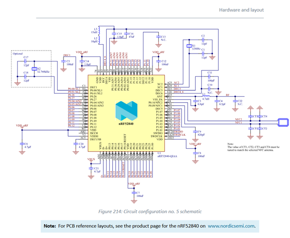
I found another schematic on google images where the VSS_PA pin is on top of the ANT pin, but don't know to what datasheet version does belong, the latest on nordic's site seems to be the v1.11.

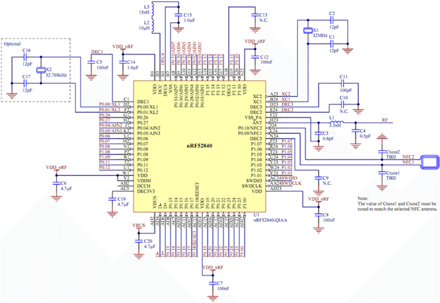
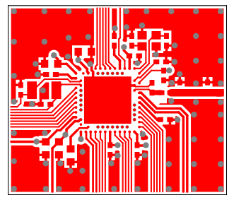
How to not get confuse by this, by looking at the PCB example?

[Oh I forgot that when we move forward to desing the PCB, the footprint has the name of the pins] 

Parents
  • Hello,

    I agree with the comment by  .

    To avoid confusion, always trust the official pinout tables and reference layouts from Nordic. The visual arrangement in a schematic or a third-party image may differ, but the pin names and numbers are definitive. When in doubt, cross-reference the pin name (e.g., ANT, VSS_PA) with the official datasheet and use the provided reference PCB layout as your guide. This will ensure your design is correct regardless of how the pins appear in different images or layouts PCB guidelines.

    Best Regards,

    Swathy

Reply
  • Hello,

    I agree with the comment by  .

    To avoid confusion, always trust the official pinout tables and reference layouts from Nordic. The visual arrangement in a schematic or a third-party image may differ, but the pin names and numbers are definitive. When in doubt, cross-reference the pin name (e.g., ANT, VSS_PA) with the official datasheet and use the provided reference PCB layout as your guide. This will ensure your design is correct regardless of how the pins appear in different images or layouts PCB guidelines.

    Best Regards,

    Swathy

Children
No Data
Related