Currently designing around the nrf54h20 and wondering if Nordic has any recommendations for properly routing the USB D+ and D- traces.
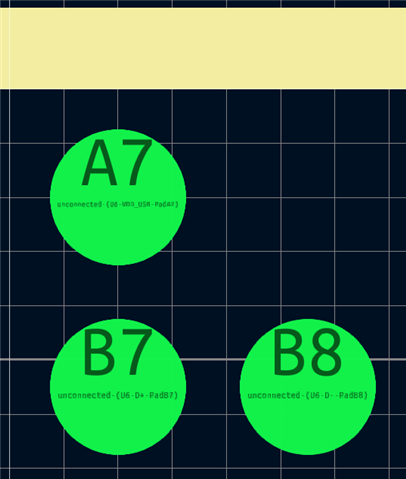
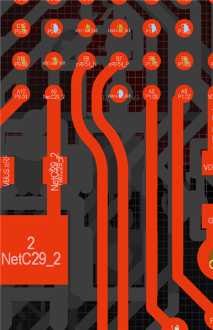
D+ and D- are supposed to be routed to pins B7 and B8, respectively. However, pin A7 blocks access to B7 on the top layer. This seems to suggest that Nordic requires us to bring D+ and D- in on an inner layer and connect using vias. However many white papers online recommend routing USB High-Speed on the top layer, avoiding the use of vias entirely. It seems this is not possible to do with the H20. If B8 we moved to A8, and B7 and A7 were switched, then D+ and D- would be on pins along the outside of the chip and accessible on the top layer.
Does Nordic have any guidance or white papers for best practices on connecting USB D+ and D- on the nrf54H20?