Solder voids under aQFN nRF52840

Hi 

We have just been notified by our supplier that they have detected som anomalies when taking X-ray images after soldering our 208 pcb's. they estimate around 25% will have unconnected pins.

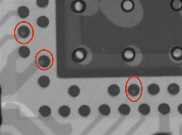
Figure1 is what our supplier calls normal.

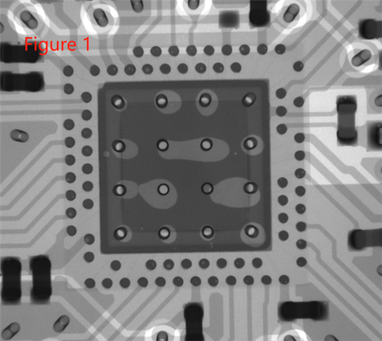
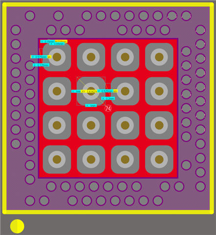
And figure 3 is with voids, where som pads dont get soldered, lucky for us they are NC.

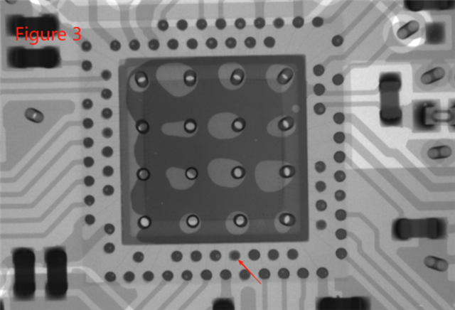
Im a HW Engineer in the field for 10years, but dont have that much knowledge about what is normal a void count/area in %, i know they what they are and can be reduced, by adjusting paste mask, solder profile, solderpaste type, etc... 

But, how many/large voids could/should be accepted? Does the number/placement of voids highlight as specific issue at our supplier? 

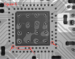
Also I'm considering changing the solder paste opening under the big centerpad to avoid that may voids in the future. (Current, OptionA, OptionB, OptionC)
CurrentOptionAOptionBOptionC

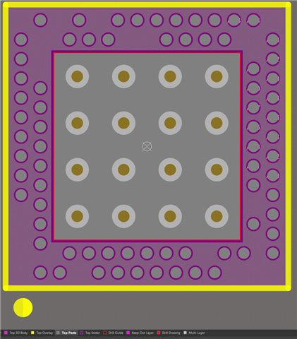
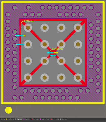
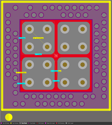
I think I would ask our supplier to use the first OptionA

Let me here you thoughts? 

Kind Regards - William

Parents
  • We're using your option A on the nRF52840-DK and other design with this device. But as far as I know, the vias are filled and plated to avoid the wicking effect of the vias. This is more important for vias in the pads than the center pad vias. 80 µm stencil thickness.

    The center pad looks in you pictures. But make sure the voids in the pads aren't getting any larger: 

    Work with the supplier with this, they know their process best.

Reply
  • We're using your option A on the nRF52840-DK and other design with this device. But as far as I know, the vias are filled and plated to avoid the wicking effect of the vias. This is more important for vias in the pads than the center pad vias. 80 µm stencil thickness.

    The center pad looks in you pictures. But make sure the voids in the pads aren't getting any larger: 

    Work with the supplier with this, they know their process best.

Children
Related