RF circuit of the 54L reference design

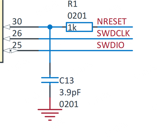
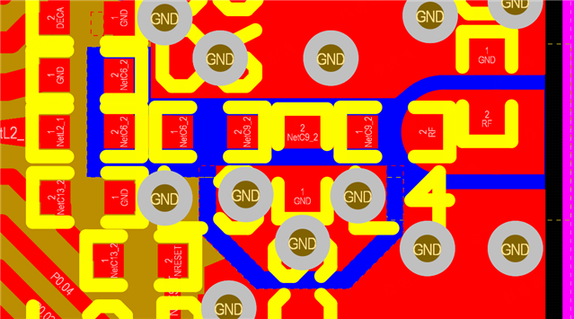
The 54L15DK has two issues. First, what is the purpose of the 3.9pF capacitor on the reset line? If it's for suppressing glitch signals, isn't the capacitance value too small? Second, the RF link is not 50 ohms. According to the DK's PCB information, with a trace width of 0.3mm, the reference layer being the fourth layer, and a board thickness of 1.6mm, achieving 50-ohm impedance is impossible. Please explain.

Parents
  • Hello,
    The RESET circuitry works in parallel to internal pull up and the component selection is simulated, tested and verified to be a good combination to prevent unintentional resets. You are welcome to test and confirm this on your board and implementation by adding noise to the reset line if this is a concern. There could be some frequencies and voltage level combination where a different capacitor value might be more suitable, but for the overall performance and implementation, this is the value we recommend.
    RF trace, the 50Ohm point is on the far right after L4. The width of the trace there is set to 0.762mm, based on the distance to GND plane on top and the GND plane on the bottom. The impedance between the components of the RF matching network is not know, only that it is 50Ohm at the output.
    Best regards
    Asbjørn
  • What is the characteristic impedance of an RF input? I need to adjust the impedance. I configured a 54L15 as the input and used a VNA to measure it. I adjusted the input to 50Ω, but the output seems unsuitable. Could you explain how to adjust it?

Reply Children
No Data
Related