Poor BLE Performance – RF Matching Guidance for nRF54L10 + nRF21540 + 2450AT18B0100001E Design

Hello,

I’m currently working on a hardware design using the following components:
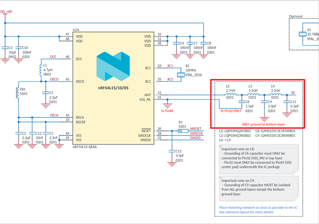
  • nRF54L10 SoC

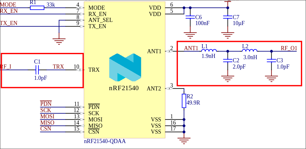
  • nRF21540 Front-End Module (FEM)

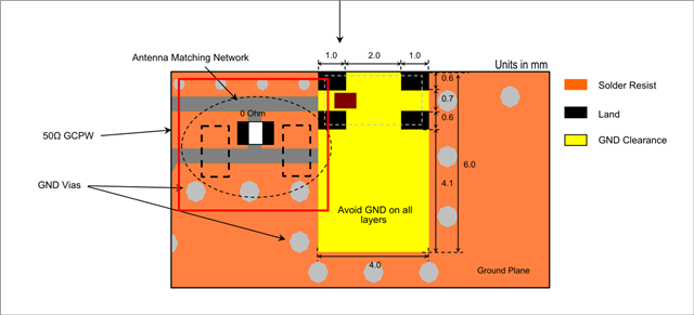
  • 2450AT18B0100001E chip antenna (Johanson Technology)

We have completed the first revision of the PCB, but we're experiencing very poor BLE performance. The signal quality is extremely low, and we suspect the issue is related to RF matching between the blocks.

Could you please provide guidance on:

  1. What kind of RF matching network should be used between:

    • nRF54L10 and nRF21540

    • nRF21540 and the 2450AT18B0100001E antenna

  2. How should the RF trace layout be implemented between each block? (e.g., impedance requirements, recommended topology, matching component suggestions)

Any reference schematics, layout examples, or application notes that could help us achieve proper matching and optimize BLE performance would be greatly appreciated.

Best regards,

Mert

Parents
  • Hi Mert,

    1.

    All the matching networks shown in the reference schematics for the nRF54L10, nRF21540 and the antenna are needed.

    2.

    All the traces between the matching networks should be impedance controlled with an impedance of 50 Ohm, the traces connection the components within the matching network does not need to be 50 Ohm. So using the reference schematics above, the trace between C11(in the nRF54L10 schematic) and C1(in the nRF21540 schematic) and the trace between C3(in the nRF21540 schematic and the first shunt capacitor in the antenna matching circuit must have an impedance of 50 Ohm.

    The antenna matching network will need to be tuned for your board, as the antenna impedance is dependent on the size and shape of the PCB.

    If you want us to review your design, and help with finding any issues with the design you can either create a new private ticket where you share your design files, or I can make this ticket private, so that you can share the design files here. 


    Best regards,

    Bendik

Reply
  • Hi Mert,

    1.

    All the matching networks shown in the reference schematics for the nRF54L10, nRF21540 and the antenna are needed.

    2.

    All the traces between the matching networks should be impedance controlled with an impedance of 50 Ohm, the traces connection the components within the matching network does not need to be 50 Ohm. So using the reference schematics above, the trace between C11(in the nRF54L10 schematic) and C1(in the nRF21540 schematic) and the trace between C3(in the nRF21540 schematic and the first shunt capacitor in the antenna matching circuit must have an impedance of 50 Ohm.

    The antenna matching network will need to be tuned for your board, as the antenna impedance is dependent on the size and shape of the PCB.

    If you want us to review your design, and help with finding any issues with the design you can either create a new private ticket where you share your design files, or I can make this ticket private, so that you can share the design files here. 


    Best regards,

    Bendik

Children
No Data
Related