nRF9151 Combined Antenna for LTE and GPS

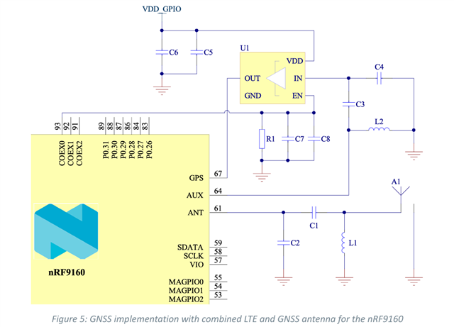
In the 'nRF91 Series Antenna and RF Interface Guidelines' document there is a section ' 4.3.1 Combined GNSS and LTE antenna example' which shows a potential way to use a single antenna for both GPS and LTE, could you please provide values for the passive components? And also with these values what frequency would the circuit operate over?

Parents
  • Hi, Bilal.

    Are you thinking of the antenna- and LNA input-matching components? If so, these values these values will differ with different antennas, LNAs, board compositions, product casings, etc., and hence, it isn't possible to provide any fixed values for these components in the datasheet.

    The antenna and LNA manufacturers might have some values provided in their datasheets, which might be good starting points, at least for the LNA, I'd suppose. My suggestion would be to check out the datasheets and/or get in touch with the manufacturers of the antenna and LNA you've chosen in order to find out if they have any reference values for these components and if they can assist you with tuning, if necessary.

    The nRF9160 SiP's GPS, AUX, and ANT pins are already matched to 50 Ω.

    Best regards,
    Mathias

  • Hi Mathias,

    Thank you for your response. I am not sure if you can see the image that I attached? The image is from the 'nRF91 Series Antenna and RF Interface Guidelines'. I understand that the matching components will vary depending on different factors but I assume that these designators have been place there for some specific design at a certain frequency? Also with the R1, C7 and C8 on the enable pin, I assume they are there for noise suppression? If you are able to share the reference design with the values that would be really helpful for me to get an idea for my design .  

Reply
  • Hi Mathias,

    Thank you for your response. I am not sure if you can see the image that I attached? The image is from the 'nRF91 Series Antenna and RF Interface Guidelines'. I understand that the matching components will vary depending on different factors but I assume that these designators have been place there for some specific design at a certain frequency? Also with the R1, C7 and C8 on the enable pin, I assume they are there for noise suppression? If you are able to share the reference design with the values that would be really helpful for me to get an idea for my design .  

Children
Related