PCB design review for my custom air quality monitor with nRF52832

Hi!

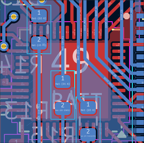
I am using the nRF52832 for a small custom PCB for a wearable device and I would appreciate a review from the experts, before proceeding with manufacturing :) 

The trickiest part is the bluetooth antenna (never designed one), so I tried to follow exactly the design in the nRF52840 dongle as this is also a 2 layer board.
And I also wanna clarify I am not expecting max performance/range nor aiming for optimal design, I just want to be able to pair this with my phone, like 1 meter range is more than okay.

Attached a zip with the gerber files and schematic pdf.
If you want the full kicad project you can download it from here.

Thanks in advance!
air-ctrl-rev1.1.zip

Parents
  • Hi,

    • C10 must be marked NC, the DEC2 pin must be floating with no decoupling capacitor
    • C19 isn't needed for the nRF52832, and can be marked NC
    • L1 should be changed to 3.9nH
    • C25 must only be grounded to the VSS pin31 and the center GND pad, and not directly to the main ground fill. This is important for the filtering of the 2nd harmonic frequency. Here is a document explaining this: 6305.nRF52 matching network.pdf
    • There is no GND vias connecting the center GND pad to the bottom layer GND fill. A minimum of 3x3 via grid should be used, this is important for the RF performance. These components and traces directly under the nRF52832 should be moved so that the vias can be added:

    Other than these points the design looks good.


    Best regards,

    Bendik

Reply
  • Hi,

    • C10 must be marked NC, the DEC2 pin must be floating with no decoupling capacitor
    • C19 isn't needed for the nRF52832, and can be marked NC
    • L1 should be changed to 3.9nH
    • C25 must only be grounded to the VSS pin31 and the center GND pad, and not directly to the main ground fill. This is important for the filtering of the 2nd harmonic frequency. Here is a document explaining this: 6305.nRF52 matching network.pdf
    • There is no GND vias connecting the center GND pad to the bottom layer GND fill. A minimum of 3x3 via grid should be used, this is important for the RF performance. These components and traces directly under the nRF52832 should be moved so that the vias can be added:

    Other than these points the design looks good.


    Best regards,

    Bendik

Children
Related