Help with UART, I2C, SPI, and I2S Pin Mapping for nRF54L05-QFAA-R (QFN48 Package)

Hello Nordic Team,

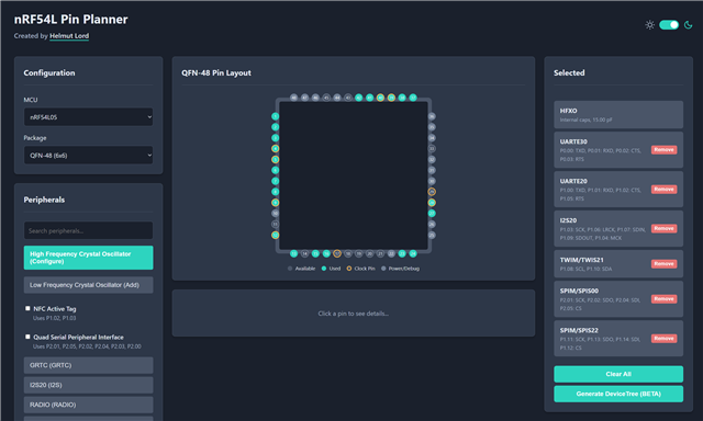
We are working with the nRF54L05-QFAA-R (QFN 48-pin package) and need clarification on which physical pins can be used for UART, I2C, SPI, and I2S interfaces.

We have reviewed the datasheet and product specification, but the pin mapping information for this specific package is not clearly defined.
It’s difficult to determine which GPIOs correspond to the available peripherals (UARTE, SPI, TWI/I2C, and I2S), and how to configure them correctly.

Our goal is to use the following peripheral setup:

  • Two UART interfaces

  • One I2C (TWI) interface

  • Two SPI interfaces

  • One I2S interface

Could you please help us with:

  1. The correct pin mapping for each of these peripherals on the QFN48 package, and

  2. Any reference documentation, pin configuration examples, or Devicetree guidance for this specific part number (nRF54L05-QFAA-R).

Thank you in advance for your support and clarification.

Best regards,
S M K Momin

Parents
  • Hello,

    Looks like it works (barely):

    It is all in the datasheet, but this is a great tool (made by one of our coworkers):

    https://pinplanner.app/

    The I2S is it's own instance, but the UARTs SPIs and I2Cs are all running on the same peripheral buses, meaning if you enable UARTE00, you can't use SPIM00 or I2C00. Since you are using 5 of these, you will be using all instances, 00, 20, 21, 22 and 30. There is also barely enough pins to get this to work. 

    You can rearrange the pins, but some pins needs to be clock pins. For reference, what I set up now to see if there were enough pins was:

    • SPIM00:
      • SCK: P2.01
      • SDO(MOSI): P2.02
      • SDI(MISO): P2.04
      • CS: P2.05
    • SPIM22:
      • SCK: P1.11
      • SDO(MOSI1.13): P
      • SDI(MISO): P1.14
      • CS: P2.05
    • UARTE20:
      • TXD: P1.00
      • RXD: P1.01
      • CTS: P1.02
      • RTS: P1.05
    • UARTE30:
      • TXD: P0.00
      • RXD: P0.01
      • CTS: P0.02
      • RTS: P0.03
    • TWIM21:
      • SCL: P1.08
      • SDA: P1.10
    • I2S20:
      • SCK: P1.03
      • LRCK: P1.06
      • SDIN: P1.07
      • SDOUT: P1.09
      • MCK: P1.04

    Does that work?

    Best regards,

    Edvin

  • Hello Edvin,

    We have configured the interfaces as per your previous input, except for I2S20. However, we noticed that SPIM00 and UARTE20 are not working with the current pin configuration.

    We then tested the following interfaces:

    • SPIM22

    • UARTE30

    • TWIM21

    All of these are working fine.

    For UARTE20, we changed the pin configuration to:

    • TXD: P1.04

    • RXD: P1.05

    With this change, it is now working correctly.

    We now need one more SPI interface for our project. Could you please suggest the proper and recommended pin configuration for an additional SPI instance?

    Thank you for your support.

    Best regards,
    S M K Momin

  • What are you testing this on? What happened when you used the UARTE pins that I suggested? And what happened to your I2S20? (which originally used P1.04 and P1.05)? Where did you place this?

    S M K Momin said:

    However, we noticed that SPIM00 and UARTE20 are not working with the current pin configuration.

    What are you testing on? The nRF54L15 DK? If so, you need to use the nRF Connect for Desktop -> "Board Configurator" to disable the default VCOMs as these are by default using the pins used for UART that are marked on the back of the DK. All the RXD, TXD, CTS, RTS pins, meaning:

    RXD0: P0.01
    TXD0: P0.00
    RTS0: P0.02
    CTS0: P0.03
    RXD1: P1.05
    TXD1: P1.04
    RTS1: P1.06
    CTS1: P1.07

    Some of these may work even if you don't disable the VCOMs/ UARTs. But these are hardwired to the debugger. If the debugger has these as an input pin, you will be fine, but e.g. the RXD0/1 will be the debugger's TXD0/1, meaning the debugger will use them as an output, and it will fight against whatever you are trying to use them for, as long as the VCOMs in "board configurator" are enabled. 

    The same applies for the P2.00 -> P2.05, used by SPIM00. If "External memory" is enabled, these pins will be disconnected from the pin headers, and connected to the external memory chip present on the DK. 

    So your setup should look like this:

    There aren't many alternative options, as you are using all the available pins, more or less. The only way to allow for more would be to disable flow control on your UARTs, if you don't need them. That leaves you with 2x2 extra gpios.

    Best regards,

    Edvin

Reply
  • What are you testing this on? What happened when you used the UARTE pins that I suggested? And what happened to your I2S20? (which originally used P1.04 and P1.05)? Where did you place this?

    S M K Momin said:

    However, we noticed that SPIM00 and UARTE20 are not working with the current pin configuration.

    What are you testing on? The nRF54L15 DK? If so, you need to use the nRF Connect for Desktop -> "Board Configurator" to disable the default VCOMs as these are by default using the pins used for UART that are marked on the back of the DK. All the RXD, TXD, CTS, RTS pins, meaning:

    RXD0: P0.01
    TXD0: P0.00
    RTS0: P0.02
    CTS0: P0.03
    RXD1: P1.05
    TXD1: P1.04
    RTS1: P1.06
    CTS1: P1.07

    Some of these may work even if you don't disable the VCOMs/ UARTs. But these are hardwired to the debugger. If the debugger has these as an input pin, you will be fine, but e.g. the RXD0/1 will be the debugger's TXD0/1, meaning the debugger will use them as an output, and it will fight against whatever you are trying to use them for, as long as the VCOMs in "board configurator" are enabled. 

    The same applies for the P2.00 -> P2.05, used by SPIM00. If "External memory" is enabled, these pins will be disconnected from the pin headers, and connected to the external memory chip present on the DK. 

    So your setup should look like this:

    There aren't many alternative options, as you are using all the available pins, more or less. The only way to allow for more would be to disable flow control on your UARTs, if you don't need them. That leaves you with 2x2 extra gpios.

    Best regards,

    Edvin

Children
  • Hi Edvin,

    Thank you so much for the detailed explanation and guidance. Your clarification about the VCOMs, UART pins, and external memory configuration on the nRF54L15 DK was extremely helpful. After following your suggestions in the Board Configurator, everything is now working as expected.

    I really appreciate your support and the clear, thorough response

    Best regards,
    SMK Momin

  • Hello,

    I am glad to hear that you got it working! 

    There is of course some flexibility. I just started in one end and populated each peripheral. You can swap some of them, but note that some peripherals requires specific clock pins. If they are selectable in the pinplanner (from the link in my initial reply) then they are compatible.

    Best regards,

    Edvin

Related