HI,
We are producing products using the nRF52832. During production, a defect occurred where the lpcomp detection voltage was operating at a voltage lower than the design voltage.
This defect occurs in approximately 5% of devices.
This issue has occurred before, and I've asked two questions, but none have been resolved.
Please refer to the previous question below for the circuit diagram and source code.
- Question 1) When detecting low battery voltage using LPCOMP and ADC, the detection voltage changes (occurs approximately 5%)
- Question 2) The reference voltage setting of lpcom does not match the calculation
I finally found a solution to a problem that kept occurring in small numbers during production.
Previously, if lpcomp was detected at "1)", the ADC for "2)" would be performed.
However, on the PCB where the lpcomp issue occurred, detecting lpcomp at "1)" and always performing ADC at "2)" allowed normal operation.
1) Read lpcomp.
nrf_lpcomp_task_trigger(NRF_LPCOMP_TASK_START);
nrf_lpcomp_task_trigger(NRF_LPCOMP_TASK_SAMPLE);
nrf_lpcomp_result_get_temp = nrf_lpcomp_result_get();
2) Stop lpcomp, process ADC once, and start again.
nrf_drv_lpcomp_disable();
temp_bat = BatVoltage();
nrf_drv_lpcomp_enable();
int32_t BatVoltage( void )
{
    int32_t BAT_output = 0;
    uint8_t channel = 0;
    nrf_saadc_value_t buf_adc;

    nrf_saadc_channel_config_t aread = {

        .resistor_p = NRF_SAADC_RESISTOR_DISABLED,
        .resistor_n = NRF_SAADC_RESISTOR_DISABLED,
        .gain       = NRF_SAADC_GAIN1_6,
        .reference   = NRF_SAADC_REFERENCE_INTERNAL,
        .acq_time   = NRF_SAADC_ACQTIME_40US,
        .mode       = NRF_SAADC_MODE_SINGLE_ENDED,
        .burst      = NRF_SAADC_BURST_DISABLED,       ///< Burst mode configuration.
        .pin_p      = NRF_SAADC_INPUT_AIN2,
        .pin_n      = NRF_SAADC_INPUT_DISABLED
    };

    nrf_saadc_channel_init( channel, &aread );
    nrf_saadc_resolution_set(SAADC_RESOLUTION_VAL_10bit);

    memset( &buf_adc, 0, sizeof(buf_adc) );
    nrf_saadc_buffer_init( &buf_adc, 1 );
    nrf_saadc_oversample_set( NRF_SAADC_OVERSAMPLE_DISABLED );
    nrf_saadc_continuous_mode_disable();

    nrf_saadc_enable();
    while( !nrf_saadc_enable_check() ){}

    nrf_saadc_task_trigger( NRF_SAADC_TASK_START );
    while( !nrf_saadc_event_check( NRF_SAADC_EVENT_STARTED ) ) {}
    nrf_saadc_event_clear( NRF_SAADC_EVENT_STARTED );

     nrf_saadc_task_trigger( NRF_SAADC_TASK_SAMPLE );
    while( !nrf_saadc_event_check( NRF_SAADC_EVENT_RESULTDONE ) ) {}
    nrf_saadc_event_clear( NRF_SAADC_EVENT_RESULTDONE );

    nrf_saadc_task_trigger( NRF_SAADC_TASK_STOP );
    while( !nrf_saadc_event_check( NRF_SAADC_EVENT_STOPPED ) ) {}
    nrf_saadc_event_clear( NRF_SAADC_EVENT_STOPPED );

    return buf_adc;

}
I don't understand why, after lpcomp operation, disabling lpcomp, doing ADC, and then enabling lpcomp again causes normal operation.
* Additionally, there are five products with identical circuitry and SW configurations, but with different PCB patterns.
However, this issue only occurs in one of the five products. The only difference is the PCB pattern.
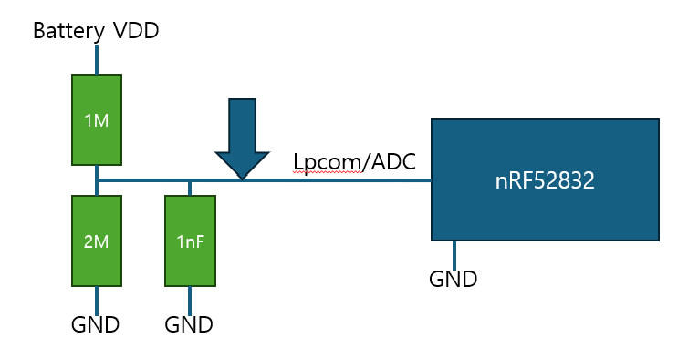
The PCBs with the pattern differences are located at 1M and 2M, and the pattern distance between the 1nF resistor and the ADC port is approximately 15cm. (The lines indicated by the arrows in the image below.)
However, the four PCBs that are functioning normally are almost directly adjacent.
Could this be the cause?