PCB antenna not scannable

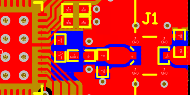
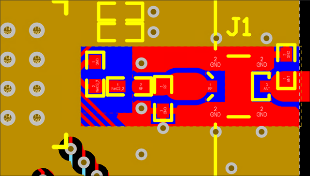
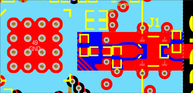
Hi, I put a PCB antenna on my nRF52832 board, designed in KiCad as closely to the reference spec as I could, and manufactured on 4 layer by JLCPCB.

With the prototype in hand, and with the example Zephyr BLE code, nRFConnect for Android scan is unfortunately not finding the device. All SPI devices are working as well as console output via RTT, just not the BLE part.

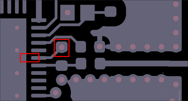
Could I have made some mistake the PCB design? Is the chip not using my crystal for some reason? I followed the reference as closely as I could in KiCad.

The schematic and PCB layout of the hardware I am testing is at this commit (some tweaks were made later but haven't been manufactured): https://github.com/wadetb/tire-sensor/commit/e5b9437c4010035f12b5f04c34cb8954465011a6

Can anyone see what I've done wrong here? And for my next revision, should I stick with this PCB antenna or is there some similar footprint prefab option that would give better performance?

Thanks for any and all advice.

Parents
  • Following up, I found several issues with the design:

    1. Ground plane under the PCB antenna. I misread the instructions to imply I needed a ground fill on the bottom layer under the entire antenna. This is removed in the latest design. The purple in the image posted is a back side coin cell battery that is locked, and KiCad is shading the locked footprint, but there is also a ground plane.

    2. When selecting my parts with JLCPCB, I accidentally allowed a substitute 40Mhz crystal in place of the 32Mhz crystal. Amazingly the device boots and all peripherals work, but this would not allow BLE to function from my understanding.

    3. Unrelated, but one of the LEDs is connected to a NC pin. D'oh

    I have an updated design, if a Nordic engineer is available to review it, the production files and KiCad sources are here:
    github.com/.../production_files

    Thanks!

  • Hi,

    There's a couple of changes needed to be the board layout:


    • There must be a GND layer directly under the SoC. It looks like there is no copper fill on L2:

      For 4 layer boards we recommend having a copper fill on L2 but with a cutout under the RF section. This cutout should also be on L3 such that the bottom layer is the reference GND plane for the transmission line. The cutout helps reduce the capacitance of the trace and component pads.  Here is some snippets showing how this should be implemented from the nRF52DK which is a 4 layer board:

      The nRF52DK hardware files can be downloaded here:
      https://www.nordicsemi.com/Products/Development-hardware/nRF52-DK/Download
    • The via grounding C3 must be removed, this capacitor should instead be grounded to the center GND pad:

      This helps increase the attenuation of the 2nd harmonic frequency.
    Other than these two points the design looks good.
     
    Best regards,
    Bendik
Reply
  • Hi,

    There's a couple of changes needed to be the board layout:


    • There must be a GND layer directly under the SoC. It looks like there is no copper fill on L2:

      For 4 layer boards we recommend having a copper fill on L2 but with a cutout under the RF section. This cutout should also be on L3 such that the bottom layer is the reference GND plane for the transmission line. The cutout helps reduce the capacitance of the trace and component pads.  Here is some snippets showing how this should be implemented from the nRF52DK which is a 4 layer board:

      The nRF52DK hardware files can be downloaded here:
      https://www.nordicsemi.com/Products/Development-hardware/nRF52-DK/Download
    • The via grounding C3 must be removed, this capacitor should instead be grounded to the center GND pad:

      This helps increase the attenuation of the 2nd harmonic frequency.
    Other than these two points the design looks good.
     
    Best regards,
    Bendik
Children
No Data
Related