nRF21540 RF FEM layout questions

Hi,

I'm designing my device based on the Thingy53 layout and I have some questions:

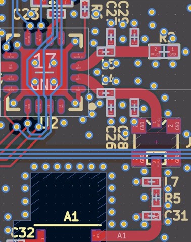
The first is why, in the T53, the antenna division comes through U17 (PE4259) instead of through the nRF21540 RF FEM?

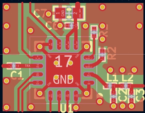
The other is, the FEM trace design in the T53 is different from the reference design indicated in the datasheet. Can you explain the reason for the changes? Why are the traces wider and why were components L5, C27 and C29 added?

Thingy53 layout:

nRF21540 FEM datasheet reference design:

Regards,

Haroldo

Parents
  • why, in the T53, the antenna division comes through U17 (PE4259) instead of through the nRF21540 RF FEM?

    From the section on Antenna selection for Thingy:53:

    The single-ended antenna output (ANT) of the nRF5340 SoC is connected to an RF switch (U17), which allows you to select either antenna A1 or antenna A2.

    Thingy:53 has two separate 2.4 GHz antennas because its RF front-end is designed to support two different transmit power paths:

    • ANT1 (high‑power path) – Connected to the nRF5340 through the nRF21540 RF front‑end module (FEM). This path provides TX gain up to +20 dBm, giving extended range and improved link robustness.

    • ANT2 (low‑power / direct path) – Connected directly from the nRF5340 through an RF switch, with TX output power up to +3 dBm, suitable for normal‑range, lower‑power operation.

    The RF switch allows the nRF5340 to use either ANT1 or ANT2 (one at a time), so applications can choose between higher range (via nRF21540) or lower power/simple operation, and comply more easily with regional RF power limits.


    why were components L5, C27 and C29 added?

    These components are added to terminate ANT2 as it is not in use. From the description of the FEM in Thingy:53 docs

    The ANT2 port of nRF21540 RF FEM is terminated to 50 Ω as recommended in the nRF21540 RF FEM reference circuitry for single antenna. The ANT_SEL pin of the nRF21540 RF FEM is therefore connected to ground.

    the FEM trace design in the T53 is different from the reference design indicated in the datasheet. Can you explain the reason for the changes?

    I have not compared the two. When designing you should make parts of the RF path a 50 Ohm coplanar waveguide. See a note on this in the guide mentioned below. All the way from the antenna matching network to where it says 'RF' in the image below should be 50 Ohm. The radio matching network itself should just have a normal signal width. Contact your PCB manufacturer in order to get the relevant parameters for calculating the width of the coplanar waveguide. In other words, the width of the path depends on the physical properties if the PCB parameters for a specific project, and these varies from project to project (trace width, copper thickness, dielectric constant in the substrate (FR4, for example) etc.

    I also recommend reading through the nRF53 General design guidelines.

Reply
  • why, in the T53, the antenna division comes through U17 (PE4259) instead of through the nRF21540 RF FEM?

    From the section on Antenna selection for Thingy:53:

    The single-ended antenna output (ANT) of the nRF5340 SoC is connected to an RF switch (U17), which allows you to select either antenna A1 or antenna A2.

    Thingy:53 has two separate 2.4 GHz antennas because its RF front-end is designed to support two different transmit power paths:

    • ANT1 (high‑power path) – Connected to the nRF5340 through the nRF21540 RF front‑end module (FEM). This path provides TX gain up to +20 dBm, giving extended range and improved link robustness.

    • ANT2 (low‑power / direct path) – Connected directly from the nRF5340 through an RF switch, with TX output power up to +3 dBm, suitable for normal‑range, lower‑power operation.

    The RF switch allows the nRF5340 to use either ANT1 or ANT2 (one at a time), so applications can choose between higher range (via nRF21540) or lower power/simple operation, and comply more easily with regional RF power limits.


    why were components L5, C27 and C29 added?

    These components are added to terminate ANT2 as it is not in use. From the description of the FEM in Thingy:53 docs

    The ANT2 port of nRF21540 RF FEM is terminated to 50 Ω as recommended in the nRF21540 RF FEM reference circuitry for single antenna. The ANT_SEL pin of the nRF21540 RF FEM is therefore connected to ground.

    the FEM trace design in the T53 is different from the reference design indicated in the datasheet. Can you explain the reason for the changes?

    I have not compared the two. When designing you should make parts of the RF path a 50 Ohm coplanar waveguide. See a note on this in the guide mentioned below. All the way from the antenna matching network to where it says 'RF' in the image below should be 50 Ohm. The radio matching network itself should just have a normal signal width. Contact your PCB manufacturer in order to get the relevant parameters for calculating the width of the coplanar waveguide. In other words, the width of the path depends on the physical properties if the PCB parameters for a specific project, and these varies from project to project (trace width, copper thickness, dielectric constant in the substrate (FR4, for example) etc.

    I also recommend reading through the nRF53 General design guidelines.

Children
Related