Can VDD and VDD_GPIO be tied to a single 3.5 V supply on nRF9151?

I am designing a very-low-cost device based on the nRF9151 and would like a quick technical clarification.

My plan is to power the SoC and all GPIO rails from a single 3.5 V supply. In the product specification, section 12.1 VDD_GPIO considerations, it states:

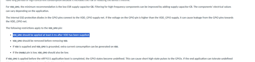
“VDD_GPIO should be applied after VDD has been supplied
VDD_GPIO should be removed before removing VDD”

My questions are:

  1. Is it permissible to connect VDD and VDD_GPIO directly together and feed them from the same 3.5 V source?

  2. If they are tied together, what negative effects, failure modes, or reliability risks should I expect (for example during power-up, power-down, brown-out, or when external GPIO devices drive pins)?

  3. Are there specific timing, voltage, or sequencing requirements I must respect that would make tying them together unsafe?

  4. Are there any recommended application notes, reference designs, or errata that address this exact use case?

For context: cost is a primary constraint — adding components is highly undesirable, so I need either confirmation that a single supply is safe

Thank you for your guidance

Parents
  • Hi,

    Regarding the VDD_GPIO considerations, you can check the below page that describes all the aspects regarding the timing and power up/down sequence:

    VDD_GPIO


    Regarding your question about powering them up from same voltage line, it is possible as the voltage you mentioned (3.5V) is within their limit, for VDD_GPIO max voltage is 3.6 V so it is on the higher end and you should make sure not to exceed that level. Regarding the timing requirements, you can have a look at Nordic Thingy 91X design to see how the power up circuit is implemented.
    Operating conditions

    Best regards,
    Ressa

Reply
  • Hi,

    Regarding the VDD_GPIO considerations, you can check the below page that describes all the aspects regarding the timing and power up/down sequence:

    VDD_GPIO


    Regarding your question about powering them up from same voltage line, it is possible as the voltage you mentioned (3.5V) is within their limit, for VDD_GPIO max voltage is 3.6 V so it is on the higher end and you should make sure not to exceed that level. Regarding the timing requirements, you can have a look at Nordic Thingy 91X design to see how the power up circuit is implemented.
    Operating conditions

    Best regards,
    Ressa

Children
Related