

I am curious about the RF pin impedance, as this parameter is not listed in the relevant specification for nRF54 SoC family (i.e. datasheet v1.0).
I wonder whether it is 50 Ohm allowing for direct antenna or amplifier connection.
I am curious about the RF pin impedance, as this parameter is not listed in the relevant specification for nRF54 SoC family (i.e. datasheet v1.0).
I wonder whether it is 50 Ohm allowing for direct antenna or amplifier connection.
Hello Sebastian,
the ANT output is not 50OHm and antenna or amplification need to be attached after the L4 and C11 where it says "RF" in the schematic.
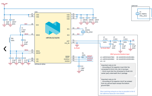
This is the 50Ohm point.
As Paal states, if you skip this, you will have a bad time with both performance and failing regulatory requirements.
Best regards
Asbjørn
Well, I assume that I can design the matching network together with antenna. So I need to know what the impedance of that pin is. Could you let me know that value, please.
Hello Sebastian,
No, please apply the reference schematic as is and then add the antenna tuning network after L4 and C11 in the schematic I attached earlier.
It is not possible to integrate the antenna input impedance matching into these components. We don't share the pin impedance because we do not want to support customers trying to do this.
Best regards
Asbjørn
In some cases, the PCB itself (material, stack-up) can impact the performance of the matching network. So it is reasonable to recalculate the circuitry. But to do so, the pin impedance is required.
Hello Sebastian,
yes, manufacturing and process can and will affect the performance and that is why we recommend to manually tune the circuit performance by changing component values on the specific board for absolute optimum performance. It will depend on the components selected as well and all effects can't be simulated. As part of our development we start with estimated values for our internal development board and then we manually tune the component values until we find the right compromise for harmonic attenuate, output power and receiver sensitivity. The outcome of this process are the values seen the in the data sheet for nRF54L15.
Best regards
Asbjørn

I also don't understand why the pin impedance can't be shared.
In the past with the nRF52, the published pin impedance meant that we could perfectly tune boards, but without this information it makes it impossible to do so.
The reason you give assumes that all customers will copy the exact specifications from your reference PCB, but this simply isn't the case. Real world designs have all shapes and sizes. The tiniest layout difference means your reference circuit will be completely off. Even something as simple as the board thickness completely de-tunes that filter. Without the pin impedance, there's no starting point for customers to re-tune from.
If the reason is because of harmonic filtering, then you need to specify the filter type, bandwidth and attenuation explicitly, such that customers can design this into their network.
As it stands, I feel the RF side of the documentation is incomplete.
I also don't understand why the pin impedance can't be shared.
In the past with the nRF52, the published pin impedance meant that we could perfectly tune boards, but without this information it makes it impossible to do so.
The reason you give assumes that all customers will copy the exact specifications from your reference PCB, but this simply isn't the case. Real world designs have all shapes and sizes. The tiniest layout difference means your reference circuit will be completely off. Even something as simple as the board thickness completely de-tunes that filter. Without the pin impedance, there's no starting point for customers to re-tune from.
If the reason is because of harmonic filtering, then you need to specify the filter type, bandwidth and attenuation explicitly, such that customers can design this into their network.
As it stands, I feel the RF side of the documentation is incomplete.

Hi,
I understand your move towards trying to reduce the burden on support, and encouraging customers to use you reference if it works in most cases. No issue there.
I don't however see why providing the pin impedance as a line in the characteristics table counteracts that.
What we do for a new radio/chip/product/package is that we will simulate a starting point with regard to component implementation and selection
This is exactly what we want to do too. It feels odd that the starting point for tuning should your lumped reference circuit rather than the source impedance itself. I'd like to challenge your claim here that the simulation never meets reality. If this is the case then something in the model is incomplete. The fact that you had to fiddle the matching network after the fact fills me with less confidence that it's accurate.
The second issue this creates, is that for us to guarantee best performance, we'd have to send all our designs through you. This shouldn't be a hoop that companies have to jump through.
I'd also like to challenge what you allude to as a "good enough" claim. I've seen a lot of customer designs that had been good enough until they realized they could have had better. On the 52 we had a lot of folks approach for tuning because they'd gone with the reference design, and then a year into production realize they should have had better range than they did. With the published impedance spec for the 52, we were easily able to improve a lot of these designs.
Today, with these specs missing, I'm down to having to probe the bare pin itself and calculate impedance from the sweep. An annoying hoop to jump through for a simple spec that should have just been provided in the first place.