
Dear Nordic-Team,
I designed a custom PCB using the nRF9151 as the host processor, the nRF7002 as a Wi-Fi companion, and the nPM1300 as the power management IC. The Wi-Fi companion is powered by a 3.3 V rail generated by an external LDO, which is enabled via the LSOUT1 output of the nPM1300. In addition, the system includes a 1.8 V power rail supplied by VOUT1 of the nPM1300.
Both the 1.8 V rail and VSYS are connected to a mechanical switch (SW1), which is used to turn the board on and off.
My pins are as follows:
| Board | nrf 9151 | nrf7002 |
| CS | P0.12 | QSPI_SS |
| SCK | P0.13 | QSPI CLK |
| MOSI | P0.14 | QSPI_DATA_0 |
| MISO | P0.15 | QSPI_DATA_1 |
| BUCKEN | P0.17 | BUCKEN |
| IRQ | P0.16 | HOST_IRQ |
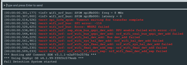
At the moment, the board is powered from a 5 V USB-C connector. When I turned on switch SW1 first, the following error message appeared:
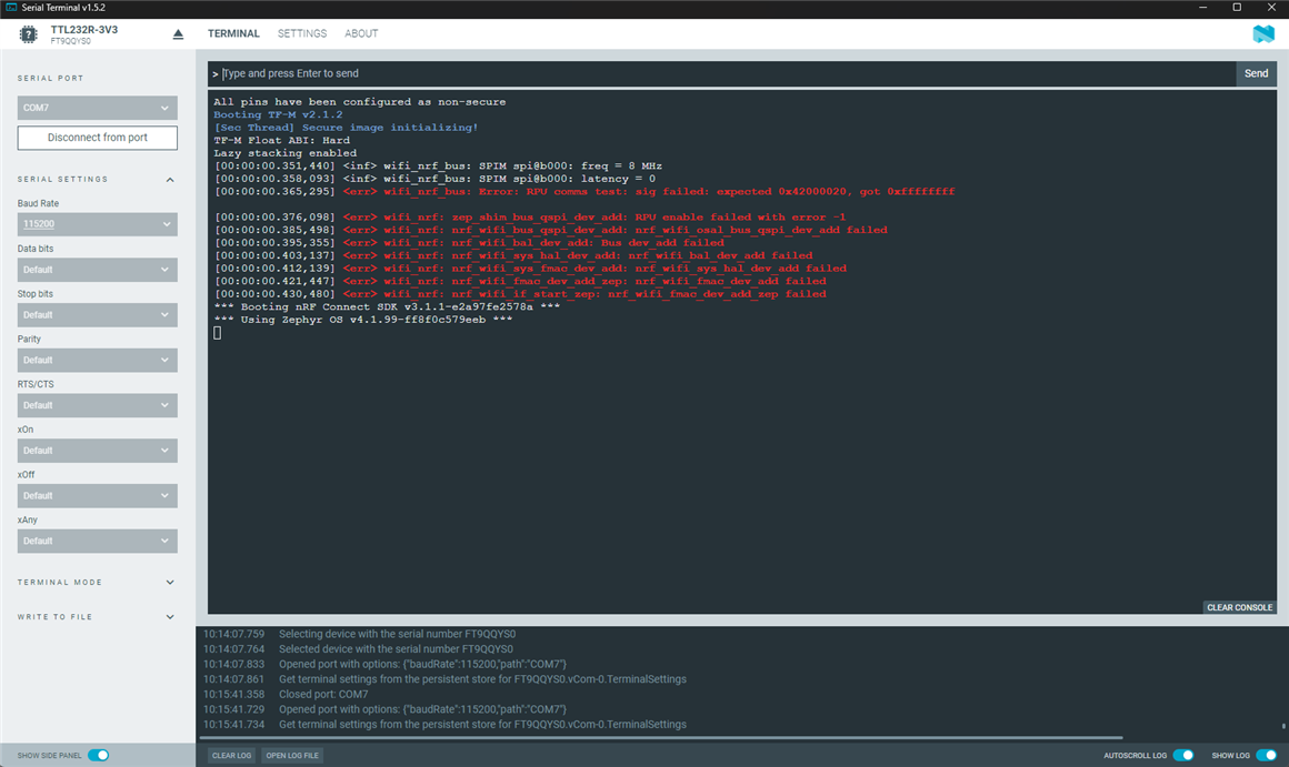
After increasing the default current limit of 100 mA of the nPM1300 to 500 mA, the original error was resolved. However, this change resulted in the following new error:
After studying once again the datasheet of the nrf7002 i found the boot up sequence which is described as follows:
14.3.5 Supply sequencing requirements
The various supplies and BUCKEN need to be sequenced in order with delay requirements.
The power up sequence and requirements are:
• Supply VBAT/BUCKVBAT/BUCKVBATS/AFEVBAT
• Wait ≥ 6 ms
• Assert BUCKEN
• Wait ≥ 1 ms
• Supply IOVDD
PWRIOVDD is an internally generated supply, used for supplying OTPVDD through an external connection.
It cannot be used for anything else. This supply is automatically controlled in the device.
The power-down sequence and requirements are:
• De-assert BUCKEN and power down IOVDD
• Power down VBAT
There are no specific timing delay requirements as long as the sequence is correct.
I realized that I did not route the IOVDD supply through a GPIO-controlled power switch from the host. Instead, IOVDD is applied immediately when SW1 is turned on. This violates the recommended power-up sequence. For my pin-ctrl gpio i am currently using GPIO P0.20 of the nrf9151 which is not routed.
My question is whether the missed boot up sequence could be the root cause of the observed error, or if there are other possible reasons that could lead to the same behavior. Since fixing the IOVDD sequencing would require hardware modifications (cutting traces and adding a switch), I would like to rule out any other potential sources of error before making such changes.
My board files are as follows:
nRF_9151_Final-pinctrl.dtsinRF_9151_Final_ns.dts
For your help i thank you already in advance.
Best wishes!
A desperate Engineer
