nRF54L15 Design Verification

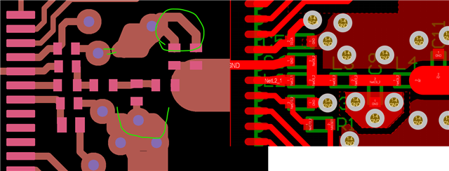
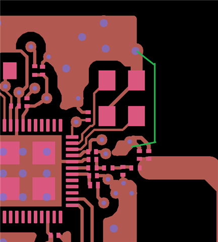
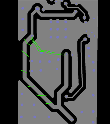
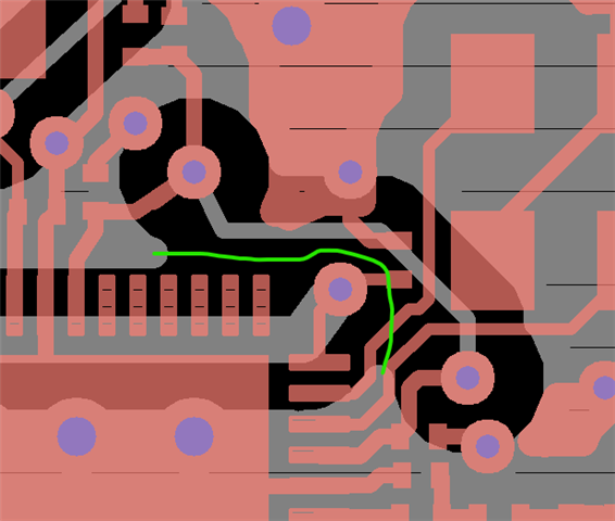
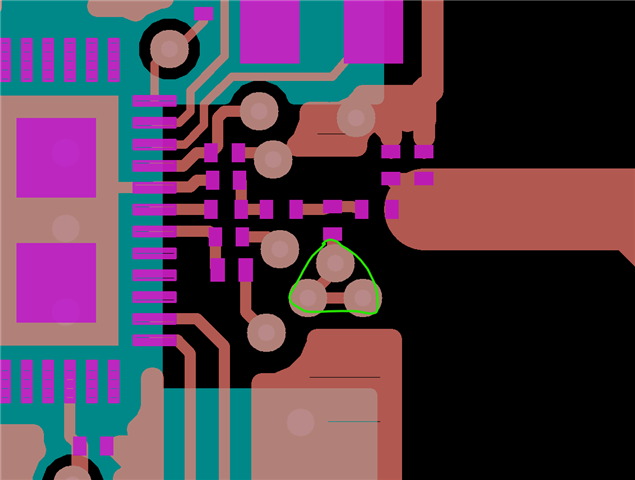
NORDIC-NRF-V1 (1).brdGERBER-SPJ_NORDIC_NRF-V1.zipNORDIC-NRF-V1 (1).schNORDIC-NRF-V1 SCHEMATIC.pdf I really need to verify this design for nrf54L15 SoC. If someone can go through it and confirm if it is okay or I need to make any changes ? I had made nRF52832 board but it did not work. So I want this design to be thoroughly verified, especially the antenna section for RF application. Awaiting replies as this has become a major bottleneck now for my projects.

  • Hi,

    I have reviewed your design, here is my feedback:

    1. L1 should be 2.7nH. The matching needs to be exactly the same as the reference design.
    2. Note: The exact value of C6 is known after antenna tuning. (It might not be needed.).
    3. C7 and C26 needs better grounding. These long traces to ground add too much impedance.
    4. Do not connect C18 ground to the top polygon, only connect it on the bottom layer. The matching network need this type of connection to suppress harmonic emissions correctly.
    5. The ground keepout on the inner layers are not actually needed, and the performance is better without them. The ground being closer to the matching shields harmonic emissions better.
    6. Ground plane should be extended further so it flows around the crystal up to the antenna. (Move the circuit to the left.) The antenna needs a continuous ground layer to work correctly.
    7. Connect the VDD trace like this: (It is not critical, but better because of lower impedance between VDD pins.)
    8. Push the DECA trace outwards so ground pour can flow between it and VDD. This creates better shielding between VDD and DECA.
    9. The right edge of the bottom GND pour is not vertical. (Not critical, purely aesthetic.)
  • Thank you so much for the response. Can you please explain why are these changes so critical for our design? Also I will make these changes and upload the files soon.

  • Hi, I have edited my reply and added the explanations in italics. I hope this clarifies things, let me know if I need to elaborate more.

  • Thank you so much. It gave me a very good insight. I have updated the design as per your suggestions. Please can you re-verify if it is okay now.GERBER-SPJ_NORDIC_NRF-V1 (1).zipNORDIC-NRF-V1.schNORDIC-NRF-V1.brd

  • Hi,

    This looks better.

    On the C18 ground pin, place a filled triangle region on the vias and the pad, like in the picture:

    With these thin traces, you are introducing parasitic inductances between the vias, which is not good.

    You can also keep the ground in the inner layers below the matching, a closer ground plane reduces the harmonic emissions. Just place a cutout around the triangle of the 3 vias.

Related