
Hello.
I'm working on a very minimalistic (function and size) board with only SWD, BLE, I2C and several GPIOs used. Since we ran into memory shortage on NRF52805, we are trying to switch to NRF54L15, but the CSP47 package is a little more problematic layout-wise. I was able to route out all other needed signals, except SWD pins, which are hidden in inner rows of pins, and cannot be routed out on TH via only board.
I would like to jump the SWD pins out through adjacent GPIOs, which will not be used on our board, physically connecting the pads, but not repurposing the pins to anything else: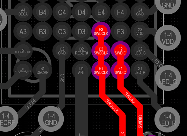
Is this generally possible, or should I expect any drawbacks?
The affected GPIOs are:
SWDIO (F2) -> P0.01 (F1)
SWDCLK (E3) -> P0.02 (E2) -> P0.03 (E1)
From what I was able to find in documentation, the GPIOs should not have a default PU/PDs associated with them, so it should not affect the SWD functionality, unless specifically changed in firmware. Specifically these sections in datasheet: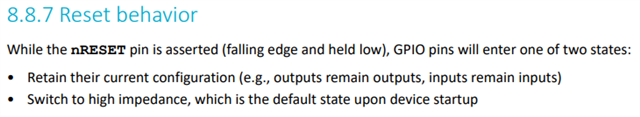
8.8.8.10 PIN_CNF default value is 0x2, ie all pins set as inputs with input buffer disconnected, no PU/PD.
Thank you.
Regards
Daniel
