
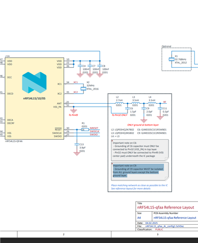
Hello, in the design reference it explicitly mentions:
“Important note on C9: The grounding of the C9 capacitor MUST be isolated from ALL ground layers except the bottom ground layer.”
However, this reference is for a 4-layer PCB. I am designing a 6-layer PCB with the following stack-up:
-
Layer 1 (Top): Signal + Components (RF, high-speed digital)
-
Layer 2 (Inner 1): Solid Ground (GND)
-
Layer 3 (Inner 2): Internal Signal Routing (Great for routing messy I2C/SPI lines without breaking ground planes)
-
Layer 4 (Inner 3): Power (VCC)
-
Layer 5 (Inner 4): Solid Ground (GND)
-
Layer 6 (Bottom): Signal + Components
What should I do with this capacitor, and where should I connect it?
Also, is there anything I need to consider in the design reference when using a different stack-up?

