
I am currently developing a project using an nRF5340DK and a custom board.
---------------------------------------------
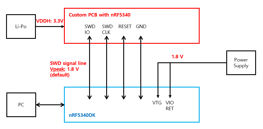
PC ---(SWD)--- IntMCU at nRF5340DK ---(SWD)--- nRF5340 on custom PCB
Custom PCB
- External 32kHz crystal: X
- External Flash memory: X
- Voltage Mode: High Voltage mode
- Internal Regulator mode: LDO
- MCU voltage: 3.3V
- MCU VDD voltage: 1.8V
- SWD signal line voltage: 1.8V (IDK why. But I input 1.8V for VIOREF pin on nRF5340DK to programm my PCB)
---------------------------------------------
However, the SWD output on the custom board is measuring at 1.8V. (This wasn't my intentional design, but it seems to be the default setting, and I proceeded without modifying it.)
To match this, I used an external power supply to provide 1.8V to the VIOREF and VTG pins of the nRF5340DK, effectively bringing the DK's SWD line voltage down to 1.8V. Debugging was proceeding smoothly with this setup.
The problem occurred during the following instances:
Occasionally, the external power supply was turned off, leaving VIOREF empty. This caused the nRF5340DK’s default 3V output to flow directly into the custom board’s RESET pin.
In other cases, SWD signals were applied to the custom board's pins while the 3.3V main power was not supplied to the board.
Current Symptoms:
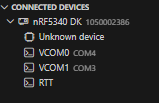
- The device is no longer detected by the nRF Connect SDK (shows as "Unknown Device").
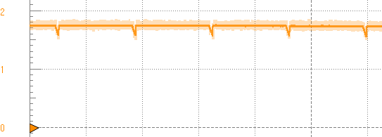
- The RESET and VDD outputs on the custom board are unstable (fluctuating).
I suspect that the incorrect voltage levels flowing through the pins have caused hardware damage.
Is there any way to recover from this, or is the chip permanently damaged?

