Hello.
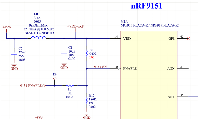
****************************** 1 ******************************
In the picture above, it's the original circuit for 9151 in our schematic, for this block of pins of the 9151. The ENABLE pin is constantly tied to level 1 by connecting ENABLE to VDD through a 10K resistor.
In this case, in the idea of this project of the picture above, the 9151 was the head/master of the PCB, so no any issues with this picture above. This was the previous board.
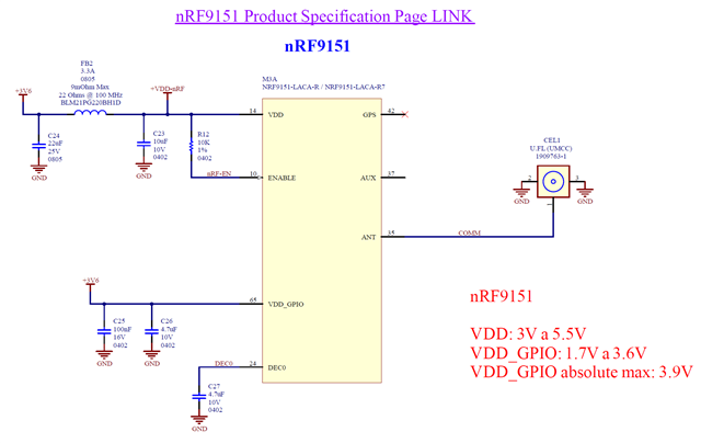
****************************** 2 ******************************
Then here begins the idea of our new and current schematic that I'm working on. It will be added to the board a module based in a 54L15. The nRF54L15 will be the head/master and the 9151 will be just a slave of the 54L15, and they would communicate via TX/RX UART, burning on the 9151 a firmware compatible with the Mosh serial terminal of Nordic. As the product is a 3.6V battery-powered, the idea is that the 54L15 stays most of time in sleep mode and be waked-up by a RTC chip at programmed horaries, and that while the 54L15 is in sleep the 9151 be disabled in hardware holding ENABLE pin of 9151 to 0 during this period. But then as we can see in this second picture, there would be a considerable consumption via resistor R13 if Q1 keeps conducting to ground.
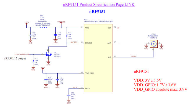
****************************** 3 ******************************
My idea was to do as in this third picture, where the ENABLE of 9151 is directly controlled by an output of 54L15, with a pull-down. Do you see any problem with this?
****************************** 4 ******************************
There is the nRESET signal of the programming interface, pin 9 of 9151, but as far as I know there is an internal pull-up on this pin, so anyway, if we hold nRESET in 0, there would be some consumption also.
****************************** 5 ******************************
Also, I would like to ask what is the typical current consumption (in uA) of 9151 when its ENABLE pin is keept tied to ground, recognizing level 0.
Regards,
Jeferson Pehls.