This post is older than 2 years and might not be relevant anymore
More Info: Consider searching for newer posts

PCB Antenna Matching Circuit for nRF8001

Hi folks,

I want to match my IFA PCB antenna to the nRF8001. As Harald recommended a couple times, I am going to measure the antenna of the final PCB with a Vector Network Analyzer, to be aware of the antennas behavior in the final built-up.

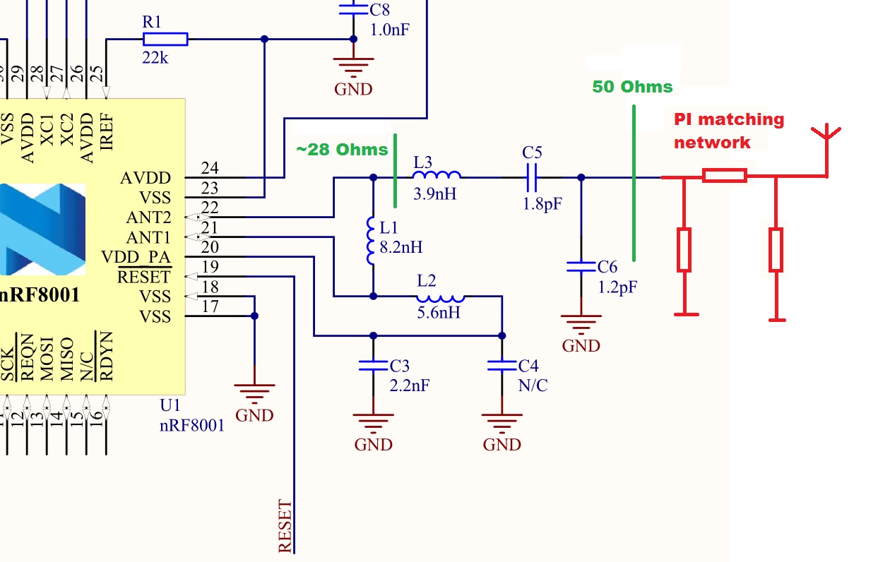
I am sure the antenna will not have a nice 50 Ohms impedance, so I wanted to add a PI matching network to the sample schematic for 50 Ohms output (marked red in the attached picture).

Assuming the antenna is matched then to 50 Ohms, I calculated the Impedance that will be seen when looking towards L3. When I calculated right, it is a nearly non complex value of around 28 Ohms (marked green in the attached picture). I calculated C6 and 50 Ohms load in parallel, all together in series with L3 and C5, omega = 15,08 GHz.

Now comes the questions: Obviously this is a bunch of components. Am I right in assuming, that it is possible to calculate equivalent impedance values between feeding point of L3 and the antenna to construct an equivalent circuit containing less components? By doing this it would be the same to get rid of L3, C5 and C6, and then to match the antenna with the PI network to 28 Ohms. Right? Or is there going to be a problem with the balun structure?

A thing thats seems strange to me: Given the 28 Ohms are correct. How does the impedance seen by the pins ANT1 and ANT2 reach the recommended value of 15+j81 Ohms for maximum output?

Thanks in advance, Carl

nrf8001_matching.jpg

  • Hi,

    The impedance seen from ANT1/ANT2 pins on nRF8001 is found from simulation, and may be a bit off due to physical layout (PCB, routing, trace width etc) The matching network has two main tasks:

    1. Filtering and suppressing harmonics/spurious.
    2. Impedance conversion (BALUN)

    A simple BALUN is quite easy to do, but combining this with a high-order filter makes things complicated. However, when you're also dealing with high frequencies in the GHz-domain, there are physical aspects that comes into play. One millimeter of trace equals ~1nH, you also have stray capacitances between your trace and ground (on both TOP and BOTTOM layer), and when you're tuning components are in the low pF/nH area, everything as a great impact on the end result.

    Now, by removing the components L3/C5/C6 you are effectively removing the sharp filter. This will cause harmonics and spurious to reach a level which is non-compliant with most teleregulatory requirements (FCC/ETSI/etc).

    Best regards Håkon

  • Hi Håkon,

    thanks for the answer. I was just afrait that it might be harmful for the nRF8001, when the impedance, that is seen by ANT1 and ANT2 differs much from the data sheets recommendation.

    I am aware of the effects I have to calculate with, when working with such high frequencies. I did the PCB design with taking care to keep the lines as short as possible. I have to consider the wires parasitic inductances as well as the capacitances towards VCC and GND and other signals. I guess there are interesting and exausting hours awaiting for me:-)

    So it seems you recommend to keep the given network, because it also works as sharp filter for the RF circuit. I will add the matching network to the given circuit then.

    Greetings, Carl

Related