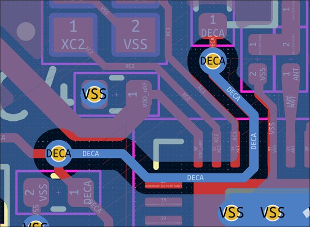
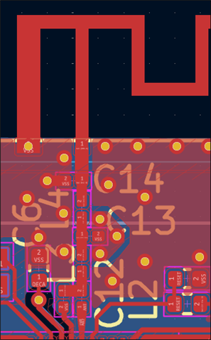
I have been working on a soil moisture sensor for my indoor plants and I wanted to build some skills in PCB design using a Nordic SoC. I have chosen the nrf54L15 for this purpose because it has BLE and is readily available at a good price. I would like the device to run on a coin cell battery and broadcast data using BLE. I have attempted to use a meandered inverted-f antenna (TI AN043: https://www.ti.com/lit/an/swra117d/swra117d.pdf) and have tried to follow the reference circuitry matching network as closely as possible. I calculated the RF trace to be 0.547 mm with a 0.13 mm gap between the ground plane and the trace. I plan to use a 0.8 mm, 2-layer board.
What I am looking for is a review of my PCB design including the RF matching network, power distribution, and general layout of components. I am only looking for ~5 m bluetooth range so I'm hoping to get away without tuning.
I have designed everything in KiCad, and have the KiCad docs on GitHub (https://github.com/bvizanko/nrf54-soil-moisture-sensor). I have attached a pdf of my schematic and a screen capture of the top layer.
Please let me know if you need clarification. Thanks!